Semiconductor memory device and its operation method

Inactive Publication Date: 2011-02-03
SONY CORP
View PDF3 Cites 15 Cited by
  • Summary
  • Abstract
  • Description
  • Claims
  • Application Information

AI Technical Summary

Benefits of technology

[0042]In accordance with the present invention, it is possible to provide a volatile or nonvolatile semiconductor memory device having a circuit configuration which is capable of making use of a simple circuit in order to carry out the next update-pulse write setting and inhibit-state setting after a read process executed as a part of a read-to-verify operation for a bit line at a high speed.
[0043]In addition, in a

Problems solved by technology

With miniaturization of the data storage element, however,

Method used


Image

  • Semiconductor memory device and its operation method
  • Semiconductor memory device and its operation method
  • Semiconductor memory device and its operation method

Examples


first embodiment

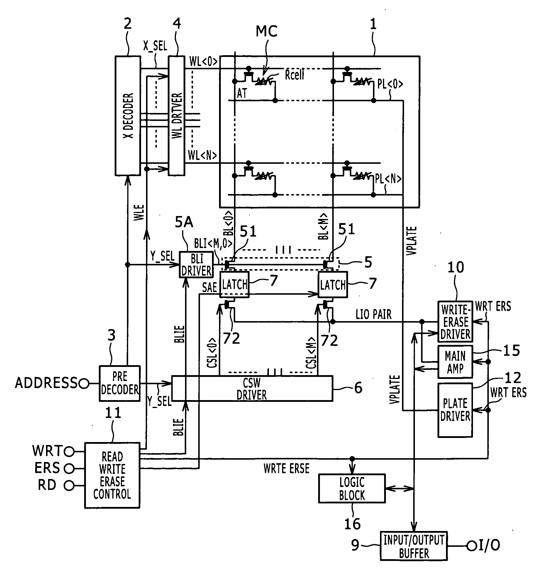
Configuration of a Memory Cell

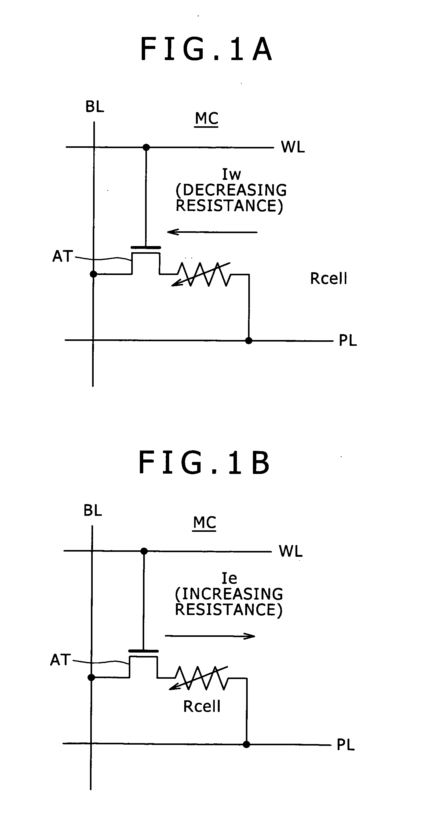
[0077]FIGS. 1A and 1B are a plurality of diagrams each showing an equivalent circuit of a memory cell MC common to embodiments of the present invention. To be more specific, FIG. 1A is a diagram particularly showing the direction of a write circuit Iw in the equivalent circuit. On the other hand, FIG. 1B is a diagram particularly showing the direction of an erase circuit Ie in the equivalent circuit. As is obvious from the diagrams of both FIGS. 1A and 1B, the memory-cell configurations themselves are identical to each other.

[0078]The memory cell MC shown in each of the diagrams of FIGS. 1A and 1B employs the variable-resistance cell resistor Rcell and an access transistor AT. Used as a data storage element, the variable-resistance cell resistor Rcell is a resistor having a variable resistance.

[0079]A specific one of the two ends of the variable-resistance cell resistor Rcell is connected to a plate line PL whereas the other one of the two ends of the v...

second embodiment

[0245]FIG. 18 is a circuit diagram showing the configurations of a column of memory cells and a BLI driver 5A which are provided in accordance with a second embodiment of the present invention. FIGS. 19A to 19K are a plurality of diagrams each showing the operation waveform (or the timing chart) of a signal for a case in which it is necessary to apply an additional data erase pulse to the memory cell MC in the event of an erase failure detected in the second embodiment. FIGS. 20A to 20K are a plurality of diagrams each showing the operation waveform (or the timing chart) of a signal for a case in which it is not necessary to apply an additional data erase pulse to the memory cell MC in the event of an erase success detected in the second embodiment.

[0246]The configuration of the column circuit shown in FIG. 18 is different from the configuration of the column circuit shown in FIG. 10 in that, the column circuit shown in FIG. 18 employs a PMOS transistor 52P in place of the NMOS tran...


PUM


Abstract

Disclosed herein is a semiconductor memory device including: a bit line and a sense line; a data storage element having a data storage state changing in accordance with a voltage applied to the bit line; a first switch for controlling connection of the sense line to the bit line; a data latch circuit having a second data holding node and a first data holding node connected to the sense line; and a second switch for controlling connection of the second data holding node of the data latch circuit to the bit line.

Description

BACKGROUND OF THE INVENTION[0001]1. Field of the Invention[0002]The present invention relates to a semiconductor memory device with its data storage state changing in accordance with a voltage applied to a bit line connected to the device and relates to a method for operating the device.[0003]2. Description of the Related Art[0004]There is known a nonvolatile memory device including a data storage element with a data storage state which changes in accordance with a voltage applied to a bit line connected to the device.[0005]Representative examples of a memory device are volatile memory devices such as DRAMs (Dynamic Random Access Memories) and SRAMs (Static Random Access Memories). Another representative example of the memory device is a nonvolatile (flash) EEPROM (Electrically Erasable Programmable Read Only Memory) represented by an FG (Floating Gate)-type memory. For more information, the reader is requested to refer to Japanese Patent No. 3142335 (hereinafter referred to as Pate...

Claims


Application Information

Patent Timeline
IPC IPC(8): G11C7/10
CPCG11C7/08G11C7/12G11C13/0011G11C13/004G11C2213/79G11C13/0069G11C2013/0073G11C2013/009G11C2211/5642G11C13/0064
Inventor KITAGAWA, MAKOTO
Owner SONY CORP
Why Eureka
Try Eureka