Two Layer Transformer

a transformer and two-layer technology, applied in transformers/inductance coils/windings/connections, electrical devices, coils, etc., can solve the problems of reducing the practical limit of the number of layers to two, and requiring at least three metal layers to create a two-layer transformer. , to achieve the effect of improving the geometrical symmetry of the structure, enhancing the geometrical symmetry, and reducing the practical limi

Active Publication Date: 2011-02-10
INTERUNIVERSITAIR MICRO ELECTRONICS CENT (IMEC VZW) +1
View PDF9 Cites 51 Cited by
  • Summary
  • Abstract
  • Description
  • Claims
  • Application Information

AI Technical Summary

Benefits of technology

[0020]In the structure of the invention, each coil has only one interconnection through the dielectric layer separating the two conductive planes, which can result in a coil with a larger inner area, and a structure with better electrical properties.
[0021]Moreover, in certain aspects of the invention, the geometry of the current structure can be easily adapted to increase the number of turns to any practical number, limited only by the available space.
[0022]In preferred embodiments, the structure of the present invention is geometrically symmetrical around three axes passing throug

Problems solved by technology

Unfortunately this structure has to be relatively large to obtain a certain inductance.
For on-chip transformers however, especially for RF applications, the practical limit of the number of layers is usually limited to two.
A disadvantage of the structures described in U.S. Pat. No. 6,870,457 is that at least three metal layers are required to create a two turn transformer.
A disadvantage of this structure is that the proposed structure having two times two turns cannot be imp

Method used


Image

  • Two Layer Transformer
  • Two Layer Transformer
  • Two Layer Transformer

Examples


example

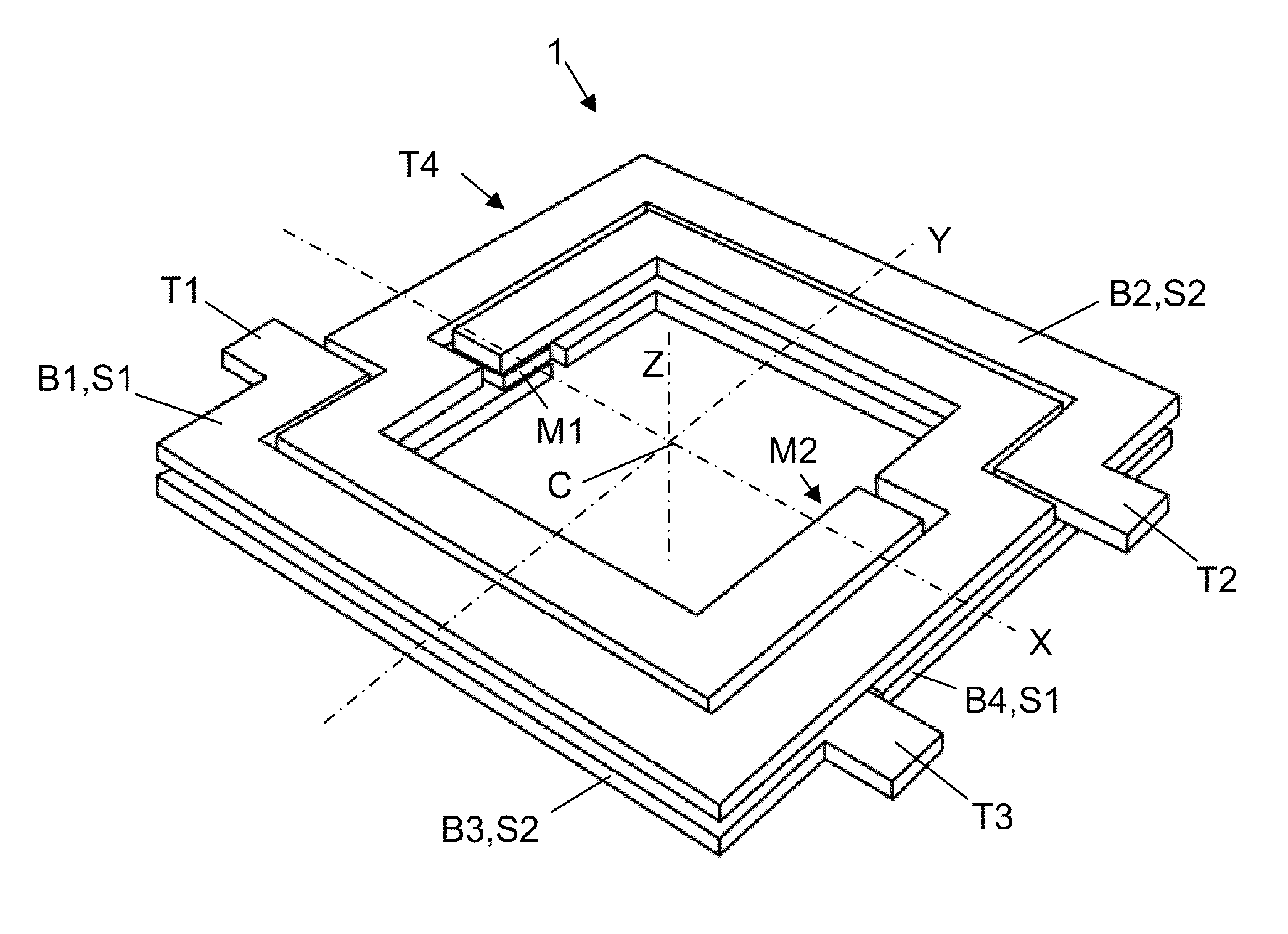
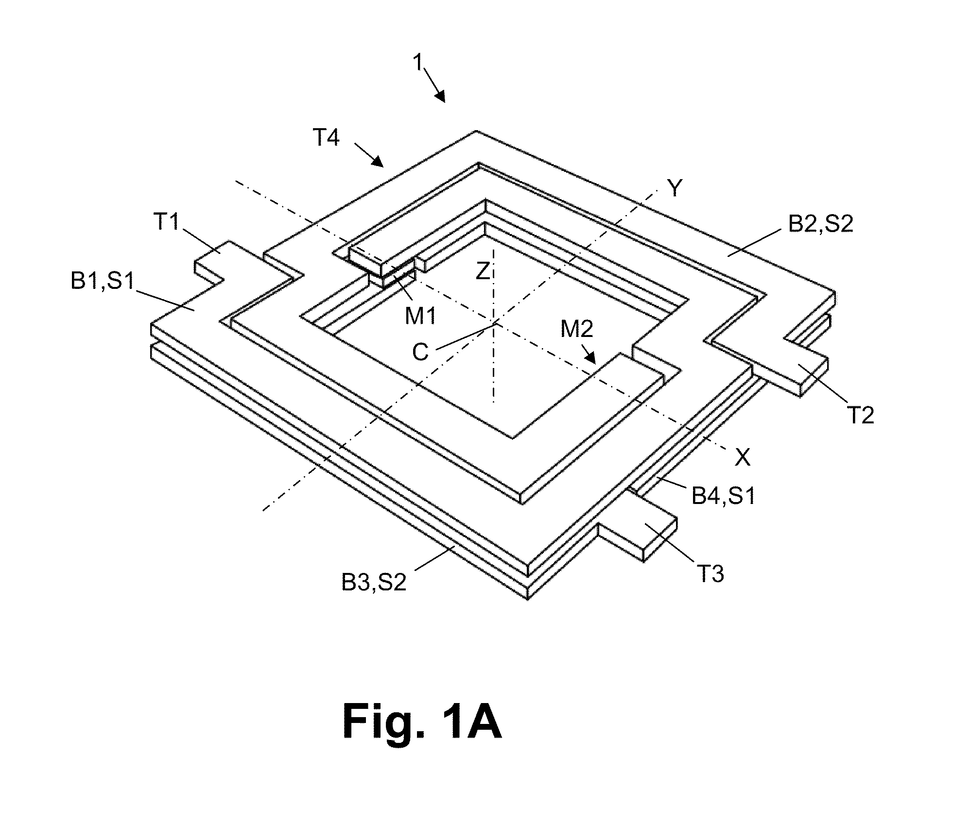
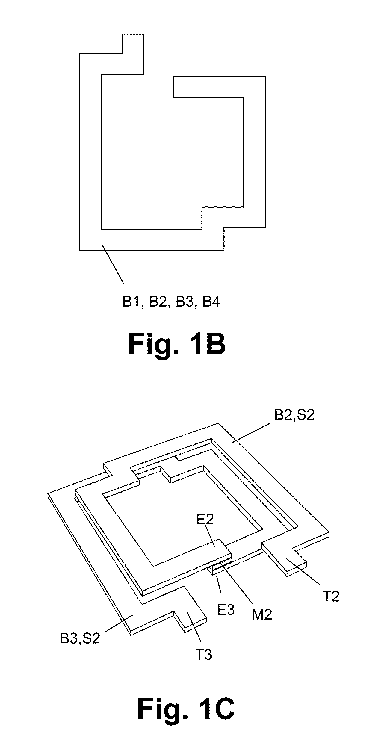
[0077]FIG. 3A shows a structure according to the invention having two coils of two windings each, in a practical 60 GHz RF chip application in CMOS technology, having the following dimensions:[0078]dimension of the outer square: 25 μm×25 μm,[0079]dimension of the inner square: 15 μm×15 μm,[0080]conductor width: 2 μm,[0081]conductor spacing: 1 μm,[0082]metal layer thicknesses T1 (FIG. 5): 0.9 μm,[0083]metal layers spacing: 0.6 μm.

[0084]However, the person skilled in the art can vary these parameters to any dimension allowed by the technology used, which can be smaller or larger than the numbers used in the simulation. For millimeter wave applications, the dimensions of the outer square could be for example 50 μm×50 μm. When the structure is implemented in a PCB layout, the distance between the metal layers could be e.g. 100 μm.

[0085]The electrical performance of the structure of FIG. 3A has been simulated, and the results are compared with a simulation of the performance of a prior a...


PUM


Abstract

One aspect of the invention relates to a symmetrical transformer with a stacked coil structure comprising two coils each having at least two turns, said coils being located in two conductive planes. The structure comprises four identical basic elements, each basic element providing a conductive path for part of said coils. The terminals of the transformer are located at opposite sites of the structure so that the structure can be easily connected in a chain.
The invention also relates to a semiconductor device comprising such a structure.

Description

CROSS-REFERENCE TO RELATED APPLICATIONS[0001]This application claims priority under 35 U.S.C. §119 to Japanese Patent Application no. 2009-185299, filed on Aug. 7, 2009, which is hereby incorporated herein by reference in its entirety.TECHNICAL FIELD OF THE INVENTION[0002]The invention relates to a symmetrical transformer with a stacked coil structure comprising a primary and a secondary coil each having at least two turns, the primary and secondary coils being located in a first and a second conductive plane which are electrically isolated from each other by an intermediate dielectric layer, the primary and secondary coils being electrically isolated from each other and being arranged so that magnetic coupling takes place between them, according to the preamble of the first claim. The invention also relates to a semiconductor device comprising such a structure.BACKGROUND OF THE INVENTION[0003]Transformers are known in the art and they are used in different types of circuits. Miniat...

Claims


Application Information

Patent Timeline
IPC IPC(8): H01F27/00H01F5/00
CPCH01F27/2804H01L23/5227H01L23/645H03H7/42H01L2924/0002H01L2924/00
Inventor RACZKOWSKI, JAKUB
Owner INTERUNIVERSITAIR MICRO ELECTRONICS CENT (IMEC VZW)
Why Eureka
Try Eureka