Optical Module and Optical Unit

Inactive Publication Date: 2011-02-10
KONICA MINOLTA OPTO
View PDF10 Cites 0 Cited by
  • Summary
  • Abstract
  • Description
  • Claims
  • Application Information

AI Technical Summary

Benefits of technology

[0015]According to the present invention, the return light reflected from the optical surface onto the light source side is diverged so that the light entering the outgoing aperture of the light source is much reduced. This arrangement eliminates the need of using a very costly high-precision positioning process and minimizes the impact of the return light upon the oscillation characteristic of a semiconductor laser.

Problems solved by technology

The semiconductor laser used as the light source of an optical module is known to be generally susceptible to return light.
This will reduce the laser gain, and will cause the relationship between the input current and laser output or the state of oscillation spectrum to be deviated from the normal characteristic range.

Method used


Image

  • Optical Module and Optical Unit
  • Optical Module and Optical Unit
  • Optical Module and Optical Unit

Examples


example 1

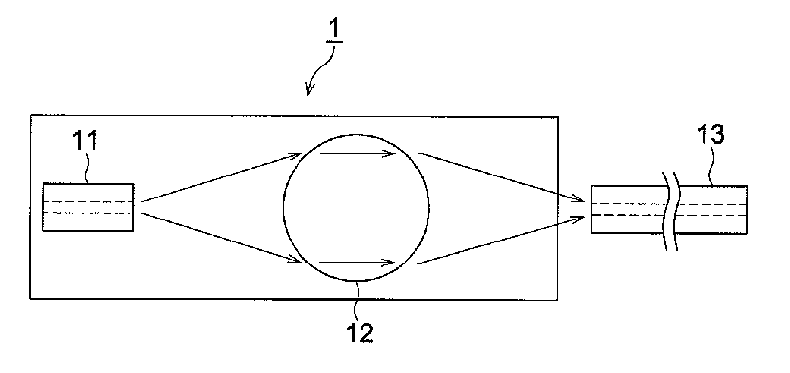
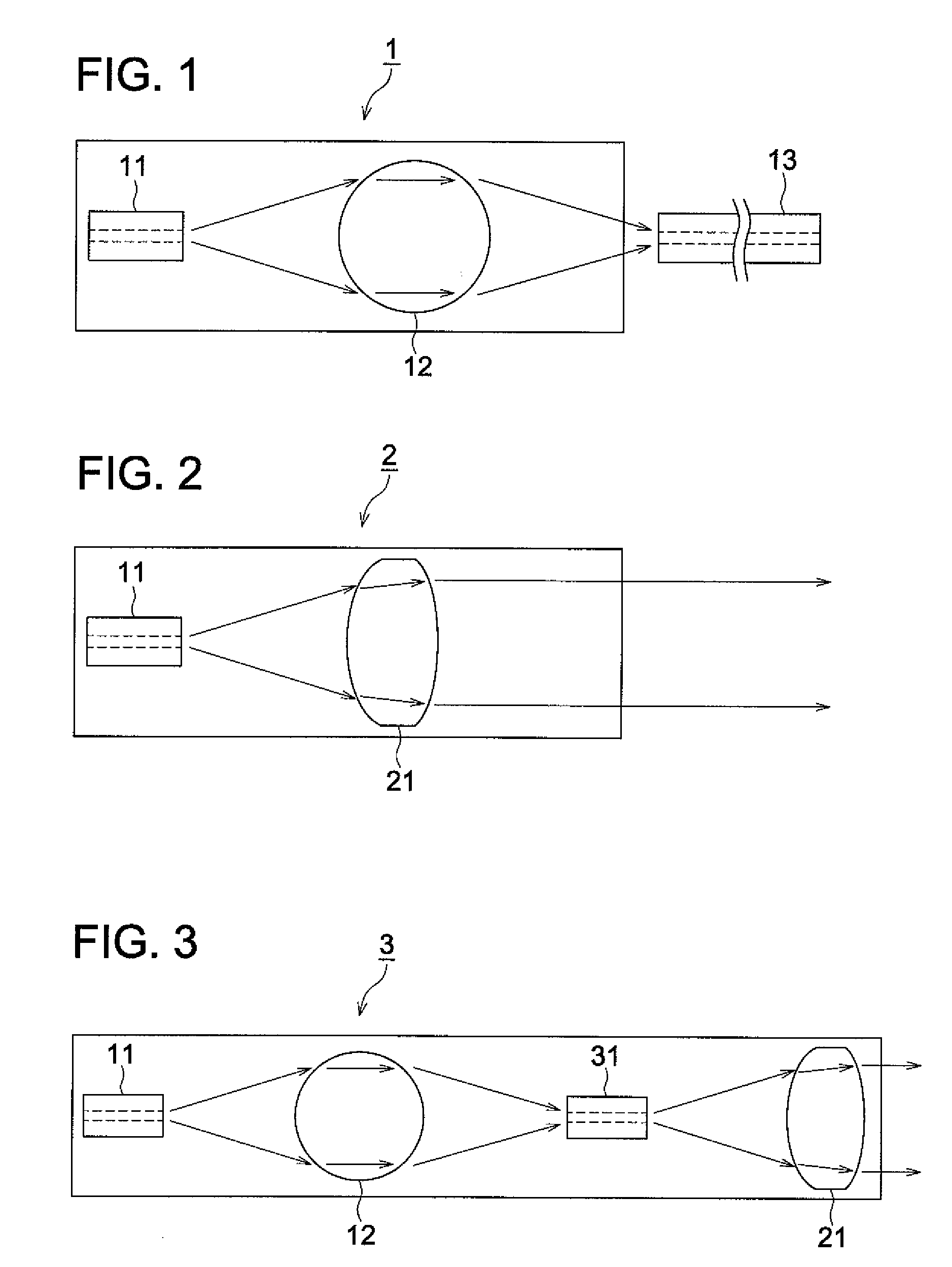
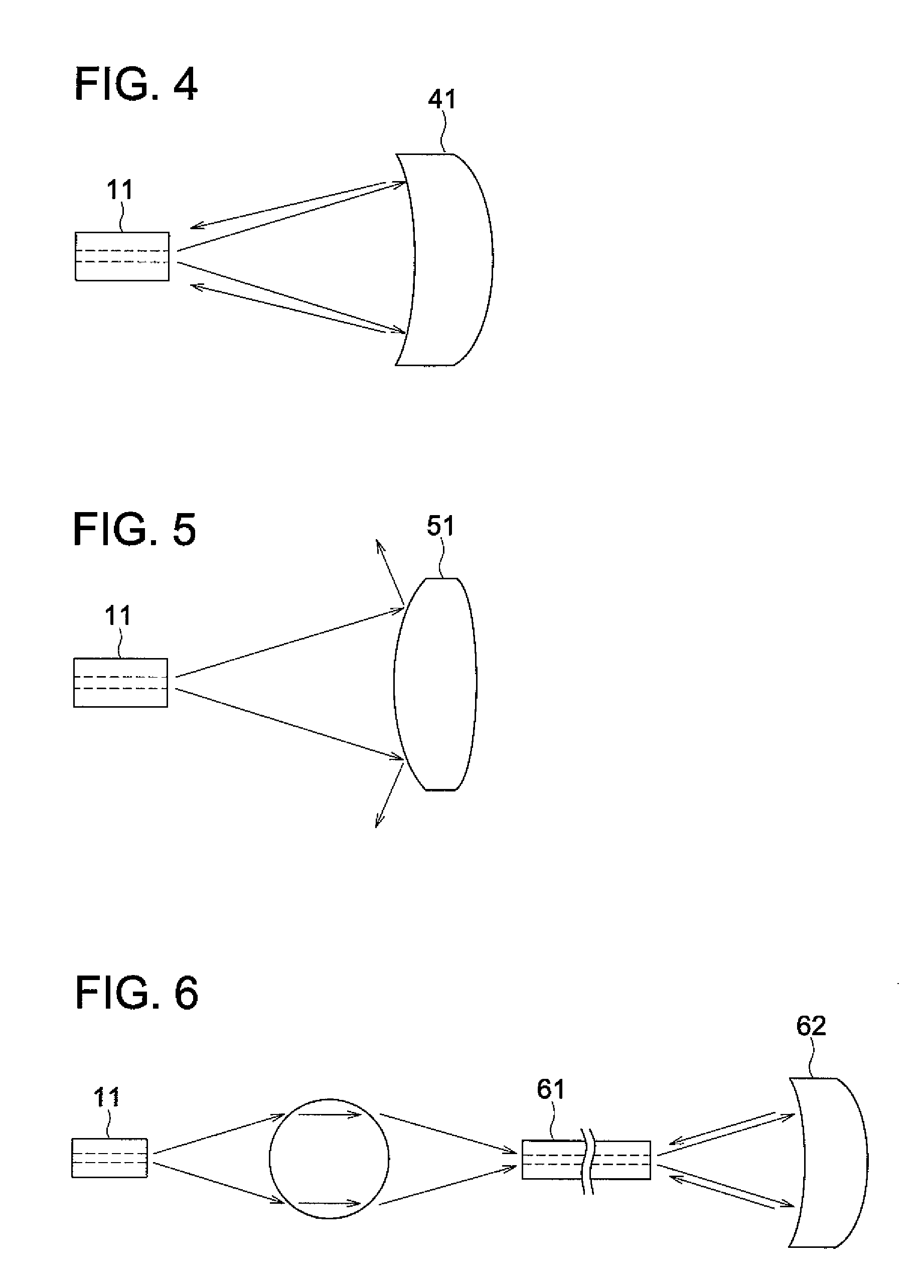
[0060]The first Example will be described. This Example represents the embodiment applicable to all of the above-mentioned first through fifth embodiments. The values shown in the optical system specification data 1 are used to represent the specifications of the optical system. The wavelength of the semiconductor laser is 1.31 μm that is used in the optical communication service. The radius in the light source mode of the optical fiber outgoing aperture is 2 μm. For example, it is possible to assume the case wherein the light emanating from the optical fiber is reflected by the optical surface of the first lens and is fed back to the optical fiber. In such a case, a collimating lens was designed to get the design result shown in the paraxial data 1 and Korenich coefficient / aspherical coefficient data 1. Here, E represents a power of ten. For example, 3.0E−01 represents 0.3. The sag Z (h) of the aspherical shape of such a lens can be expressed by the following Mathematical Formula 1...

example 2

[0071]The following describes the second Example. This Example represents the embodiment applicable to all of the above-mentioned first through fifth embodiments. For example, it is possible to assume the case wherein the light emanating from the semiconductor laser is reflected by the optical surface of the first lens and is fed back to the optical fiber. The values shown in the optical system specification data 1 are used to represent the specifications of the optical system. When “Z” is assumed to represent the traveling direction of light, the mode radius in the outgoing aperture is 2 μm in the direction X, and 3 μm in the direction Y. In the semiconductor laser, the light confinement effects are different between the directions X and Y. Thus, the mode radiuses are also different between the directions X and Y. The wavelength of the light source is 1.06 μm. In such a case, a collimating lens was designed to get the design result shown in the paraxial data 2 and Korenich coeffici...

example 3

[0076]The following describes the third Example. This Example represents the embodiment applicable to all of the above-mentioned first through fifth embodiments. The values shown in the optical system specification data 3 are used to represent the specifications of the optical system. The wavelength of the light source is 1.31 μm that is used in optical communication services. The mode radius of the optical fiber outgoing aperture is 10 μm. For example, it is possible to assume the case wherein the light emanating from the optical fiber is reflected by the optical surface of the first lens and is fed back to the optical fiber. In such a case, a collimating lens was designed to get the design result shown in the paraxial data 3 and Korenich coefficient / aspherical coefficient data 3.

[0077]The on-axis spherical aberration of the designed lens is 1 mλrms, as shown in the design result data 2. This value is sufficiently capable of standing up to commercial use as a collimating lens for u...


PUM


Abstract

A semiconductor laser used as a light source of an optical module is susceptible to the return light from the lens surface. The problem has been conventionally solved by offsetting the optical axis of a lens and the optical axis of a semiconductor laser, but a high-precision and costly process for adjusting the positioning is required. An optical module and an optical unit, wherein the oscillation state of a semiconductor laser can be limited in the range of normal characteristics at a low cost, are provided by proposing a lens which eliminates the need for adjusting the positioning because there is little return light. As a first lens on which the light exiting a semiconductor laser impinges at first, a lens having an optical surface whose convex surface faces toward the semiconductor laser side is employed so that the light is diverged thus reducing the intensity of light returning to the semiconductor laser.

Description

FIELD OF THE INVENTION[0001]The present invention relates to an optical module and optical unit that join light of a laser light source to an optical fiber, emit the light to a space, or apply such processing as modulation or conversion of wavelength to the light.BACKGROUND OF THE INVENTION[0002]The semiconductor laser used as the light source of an optical module is known to be generally susceptible to return light. If light passes through some path to return to the active layer wherein the semiconductor laser is in the state of oscillation, the return light causes stimulated emission. This will reduce the laser gain, and will cause the relationship between the input current and laser output or the state of oscillation spectrum to be deviated from the normal characteristic range. Thus, to maintain the oscillation state of the semiconductor laser within the normal characteristic range, it has been essential to minimize the input of return light in the conventional art.[0003]The coun...

Claims


Application Information

Patent Timeline
IPC IPC(8): G02B27/18H01S3/00
CPCG02B6/4207H01S5/02284H01S5/0064H01S5/02251
Inventor NAGAI, FUMIO
Owner KONICA MINOLTA OPTO
Why Eureka
Try Eureka