
VLSI layouts of fully connected generalized networks

a technology of fully connected generalized networks and layouts, applied in the direction of denominational number representation, instruments, pulse techniques, etc., can solve the problems of inefficient and simple direct embedding of a generalized multi-stage network on to a 2d mesh network, and achieve the effects of reducing signal latency, reducing power consumption, and reducing cross points

Active Publication Date: 2011-02-17
KONDA VENKAT
View PDF18 Cites 23 Cited by
  • Summary
  • Abstract
  • Description
  • Claims
  • Application Information

AI Technical Summary

Benefits of technology

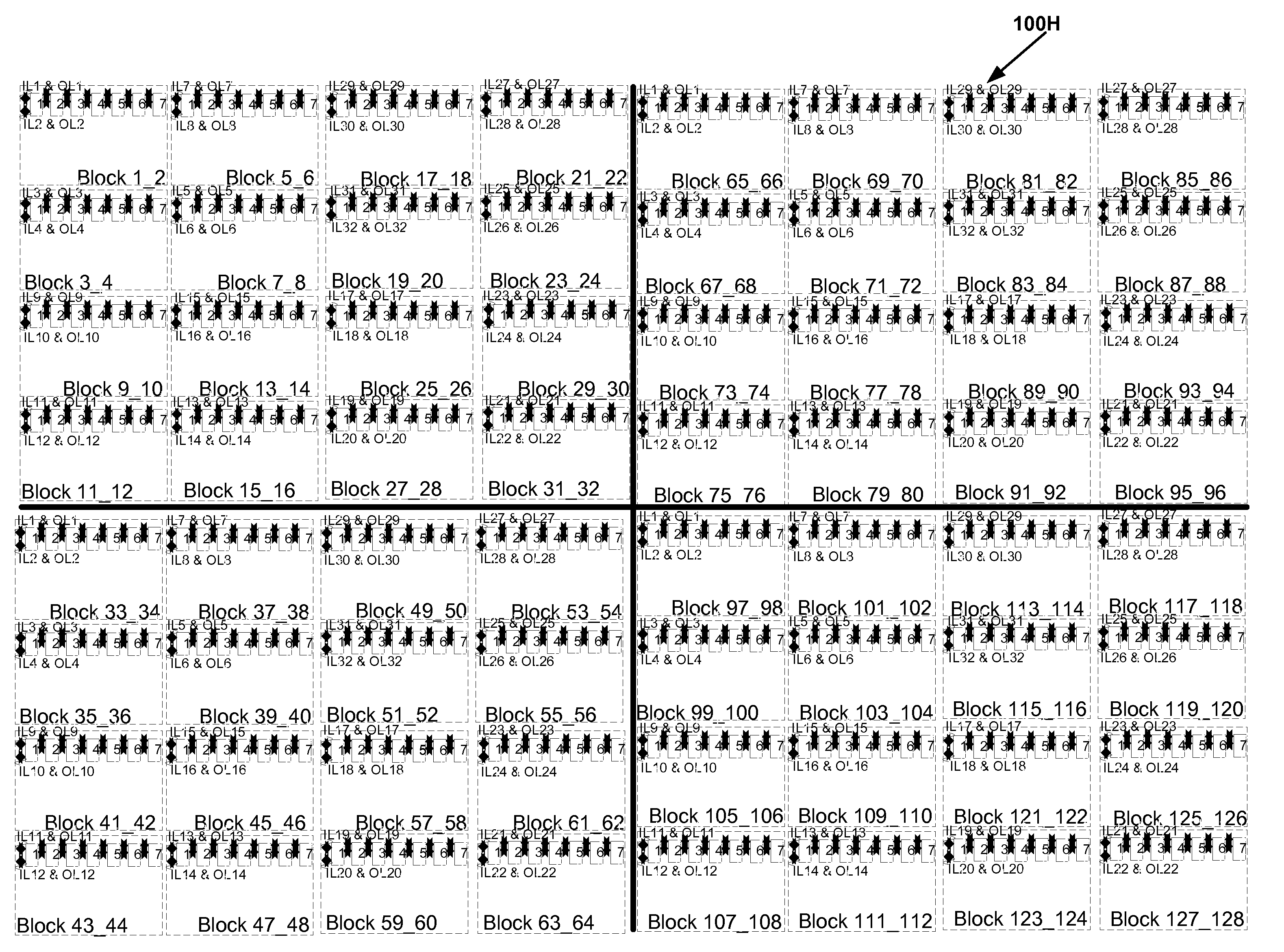
"The invention presents a method for efficiently routing connections in an integrated circuit device using a two-dimensional grid arrangement of large scale sub-integrated circuit blocks. The method uses a network of shuffle exchange links between switches in different sub-integrated circuit blocks to connect vertical and horizontal links. The layouts are applicable to various types of networks and can be used in a wide range of applications. The technical effects include lower signal latency, lower power consumption, and full connectivity with fast compilation."

Problems solved by technology

A direct embedding of a generalized multi-stage network on to a 2D Mesh network is neither simple nor efficient.

Method used


Image

  • VLSI layouts of fully connected generalized networks
  • VLSI layouts of fully connected generalized networks
  • VLSI layouts of fully connected generalized networks

Examples


Embodiment Construction

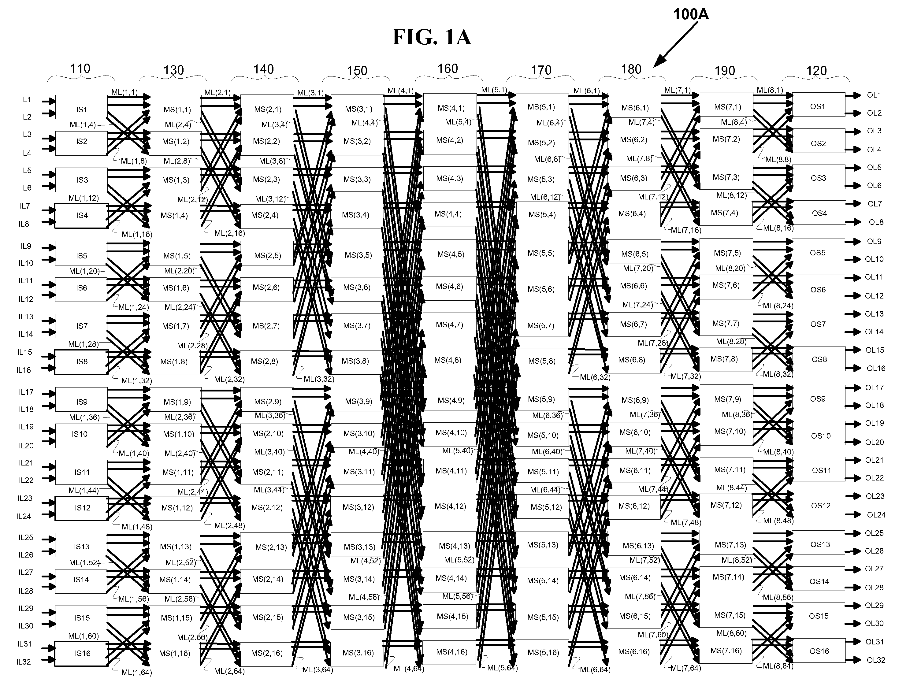
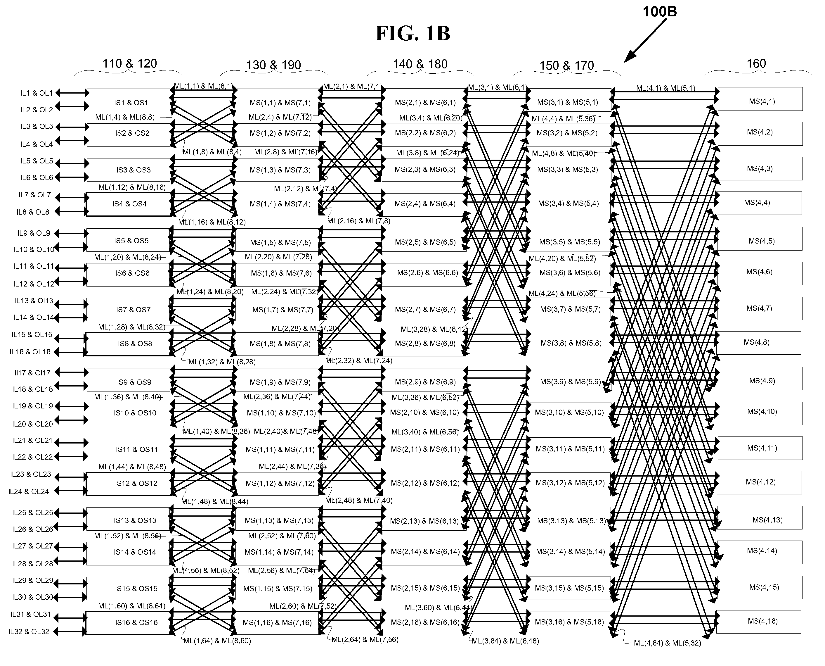
[0054]The present invention is concerned with the VLSI layouts of arbitrarily large switching networks for broadcast, unicast and multicast connections. Particularly switching networks considered in the current invention include: generalized multi-stage networks V(N1, N2, d, s), generalized folded multi-stage networks Vfold(N1, N2, d, s), generalized butterfly fat tree networks Vbft(N1, N2, d, s), generalized multi-link multi-stage networks Vmlink(N1, N2, d, s), generalized folded multi-link multi-stage networks Vfold-mlink(N1, N2, d, s), generalized multi-link butterfly fat tree networks Vmlink-bft(N1, N2, d, s), and generalized hypercube networks Vhcube(N1, N2, d, s) for s=1, 2, 3 or any number in general.

[0055]Efficient VLSI layout of networks on a semiconductor chip are very important and greatly influence many important design parameters such as the area taken up by the network on the chip, total number of wires, length of the wires, latency of the signals, capacitance and henc...


PUM


Abstract

In accordance with the invention, VLSI layouts of generalized multi-stage networks for broadcast, unicast and multicast connections are presented using only horizontal and vertical links. The VLSI layouts employ shuffle exchange links where outlet links of cross links from switches in a stage in one sub-integrated circuit block are connected to inlet links of switches in the succeeding stage in another sub-integrated circuit block so that said cross links are either vertical links or horizontal and vice versa. In one embodiment the sub-integrated circuit blocks are arranged in a hypercube arrangement in a two-dimensional plane. The VLSI layouts exploit the benefits of significantly lower cross points, lower signal latency, lower power and full connectivity with significantly fast compilation.The VLSI layouts presented are applicable to generalized multi-stage networks V(N1, N2, d, s), generalized folded multi-stage networks Vfold(N1, N2, d, s), generalized butterfly fat tree networks Vbft(N1, N2, d, s), generalized multi-link multi-stage networks Vmlink(N1, N2, d, s), generalized folded multi-link multi-stage networks Vfold-mlink(N1, N2, d, s), generalized multi-link butterfly fat tree networks Vmlink-bft(N1, N2, d, s), and generalized hypercube networks Vhcube(N1, N2, d, s) for s=1, 2, 3 or any number in general. The embodiments of VLSI layouts are useful in wide target applications such as FPGAs, CPLDs, pSoCs, ASIC placement and route tools, networking applications, parallel & distributed computing, and reconfigurable computing.

Description

CROSS REFERENCE TO RELATED APPLICATIONS[0001]This application is related to and claims priority of the PCT Application Serial No. PCT / US08 / 64605 entitled “VLSI LAYOUTS OF FULLY CONNECTED GENERALIZED NETWORKS” by Venkat Konda assigned to the same assignee as the current application, filed May 22, 2008, and the U.S. Provisional Patent Application Ser. No. 60 / 940,394 entitled “VLSI LAYOUTS OF FULLY CONNECTED GENERALIZED NETWORKS” by Venkat Konda assigned to the same assignee as the current application, filed May 25, 2007.[0002]This application is related to and incorporates by reference in its entirety the U.S. application Ser. No. 12 / 530,207 entitled “FULLY CONNECTED GENERALIZED MULTI-STAGE NETWORKS” by Venkat Konda assigned to the same assignee as the current application, filed Sep. 6, 2009, the PCT Application Serial No. PCT / US08 / 56064 entitled “FULLY CONNECTED GENERALIZED MULTI-STAGE NETWORKS” by Venkat Konda assigned to the same assignee as the current application, filed Mar. 6, 2...

Claims


Application Information

Patent Timeline
Patent Type & Authority Applications(United States)
IPC IPC(8): H01L25/00
CPCG06F17/5077G06F30/394
Inventor KONDA, VENKAT
Owner KONDA VENKAT
Learn More