Gate drive voltage boost schemes for memory array II

a technology of gate drive voltage and memory array, which is applied in the direction of information storage, static storage, digital storage, etc., can solve the problems of significant reduction of achieve the effect of reducing the life of the cell transistor, high programming current, and high memory cell curren

Active Publication Date: 2011-02-17
TAIWAN SEMICON MFG CO LTD
View PDF11 Cites 1 Cited by
  • Summary
  • Abstract
  • Description
  • Claims
  • Application Information

AI Technical Summary

Benefits of technology

[0008]Magnetic memory elements using the Giant magneto-resistive effect, such as Phase Change RAM and Spin Moment Transfer MRAM, sometimes referred to as Spin Torque Transfer MRAM, require high programming currents. Since these currents are controlled by a cell transistor, which is

Problems solved by technology

This high gate to source/drain voltage and high memory cell cu

Method used


Image

  • Gate drive voltage boost schemes for memory array II
  • Gate drive voltage boost schemes for memory array II
  • Gate drive voltage boost schemes for memory array II

Examples


Embodiment Construction

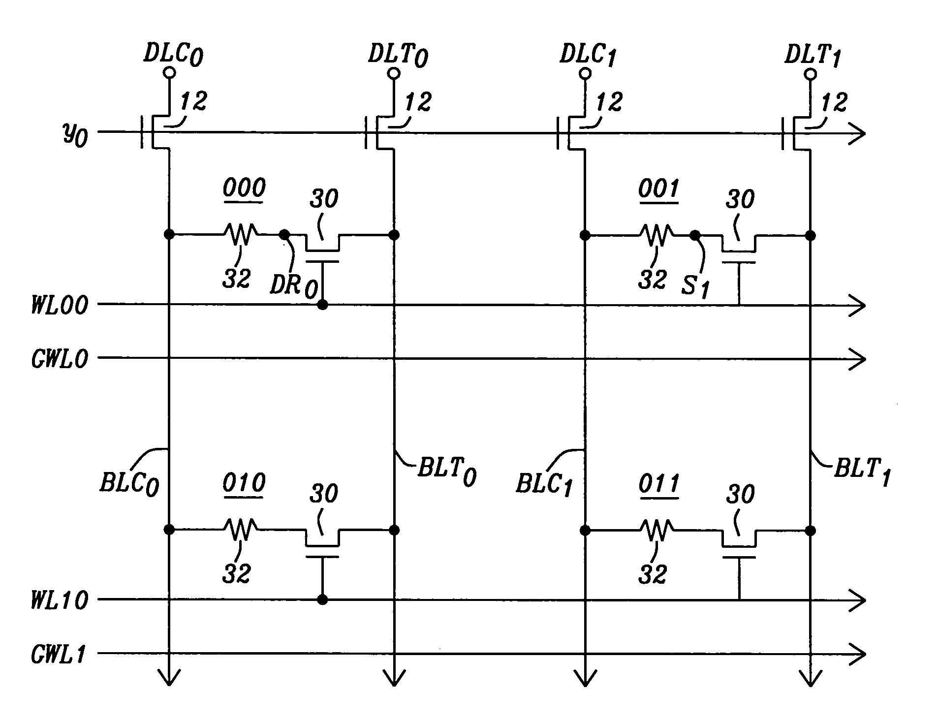
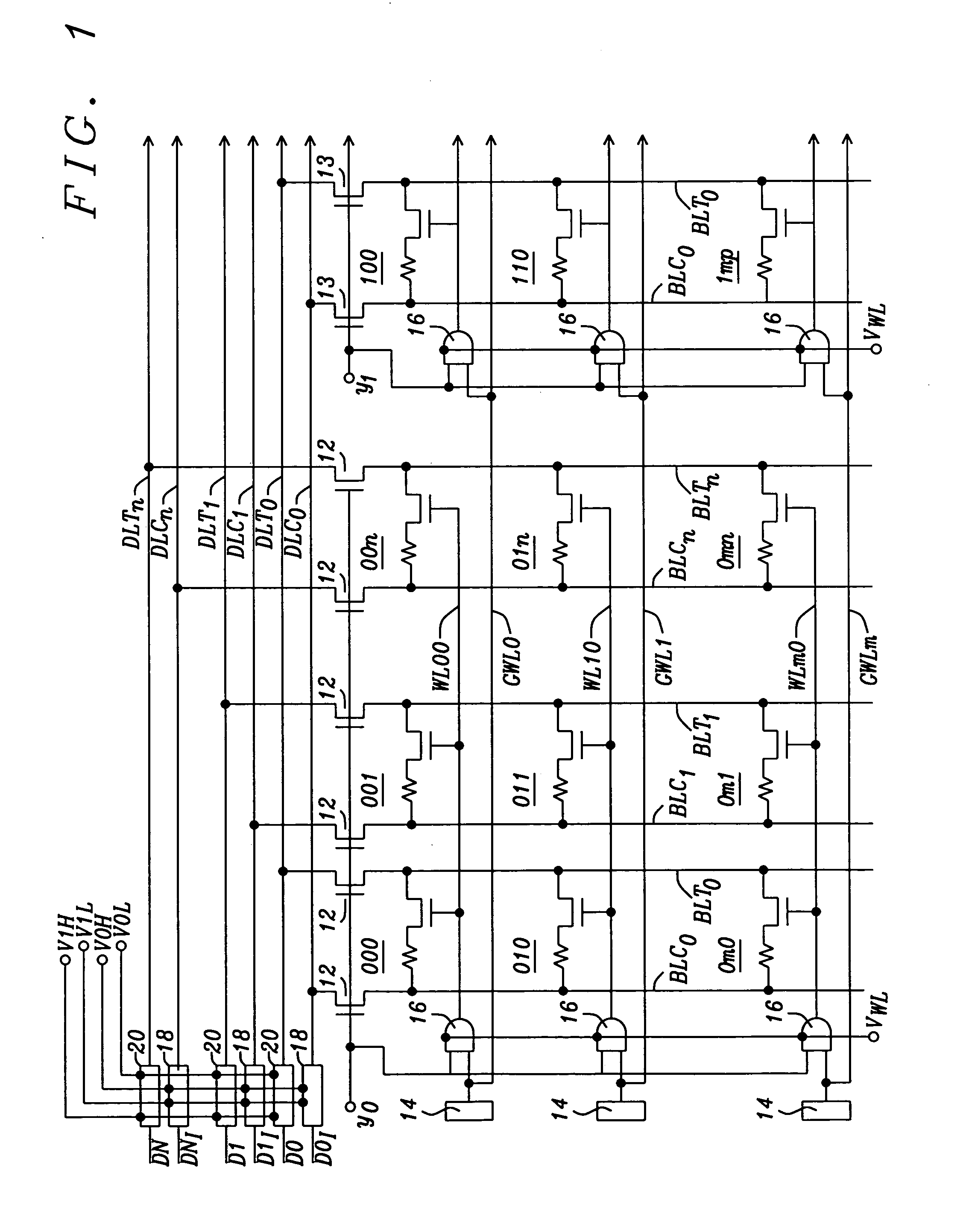
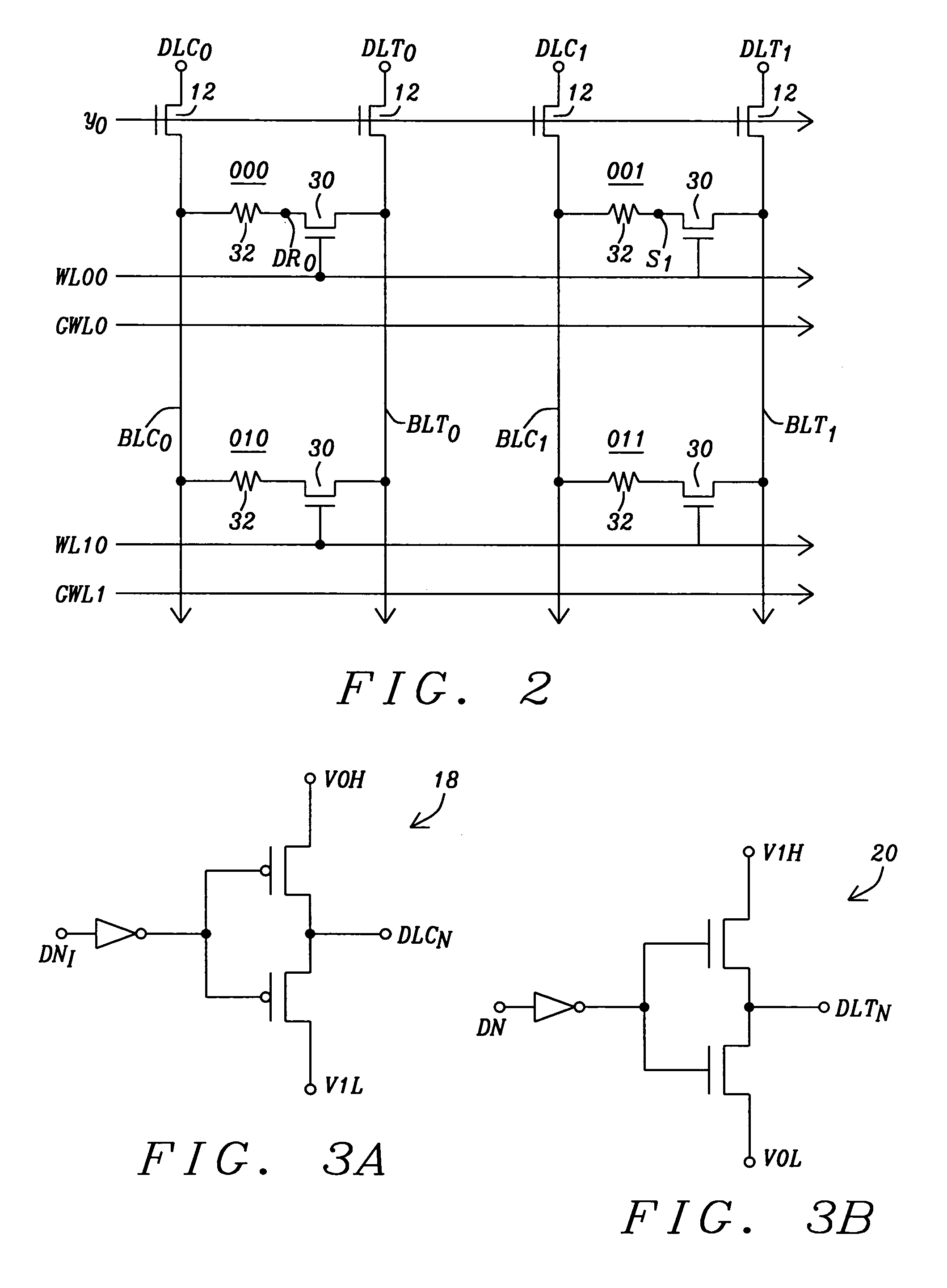
[0017]Refer now to the Drawings for a description of the preferred embodiments of this invention. FIG. 1 shows one section, section 0, of a magnetic memory comprising an n column by m row array of magnetic memory cells 000, 001, . . . , 00n, 010, 011, . . . , 01n, 0m0, 0m, . . . 0mn. FIG. 1 also shows the beginning of another section, section 1, of the magnetic memory showing magnetic memory cells 110, 111, . . . , 1m0. This description will describe the example of section 0, as those skilled in the art will readily understand how the invention is applied to other sections as they are selected. FIG. 2 shows a schematic diagram of memory cells 000, 001, 010, and 011 showing each memory cell having a cell transistor 30 and a magnetic memory element 32 with one terminal of the magnetic memory element 32 connected to one of the source / drain terminals of the cell transistor 30. In FIG. 2 this node between the cell transistor 30 and magnetic memory element 32 is designated by the referenc...


PUM


Abstract

Magnetic memory elements such as Phase Change RAM and Spin Moment Transfer MRAM require high programming currents. These high programming currents require high gate to source/drain voltages for the cell transistors controlling these programming currents, which can degrade the reliability of these cell transistors. This invention describes a circuit and method to write information into individual memory cells while minimizing the gate voltage stress in the cell transistors of the memory cells in which no information is being written. The circuit of this invention has a separately controllable word line voltage supply for each row of the memory array and a separately controllable voltage supply for each bit line of the memory array. During the write operation the voltage is raised for the word line of only one row of the array. The bit line voltages are then adjusted so that a 1 is written into the desired cells in that row and a 0 is written into the desired cells in that row.

Description

BACKGROUND OF THE INVENTION[0001](1) Field of the Invention[0002]This invention relates to gate drive voltage for magnetic memory technologies, such as Phase Change RAM and Spin Moment Transfer MRAM, sometimes referred to as Spin Torque Transfer MRAM, cells which require programming currents higher than the minimum cell transistor can provide without degrading the life of the cell transistor. More particularly the invention relates to circuits and methods for programming these cell transistors by applying high voltages between the gate and source or drain of the cell transistor only to those cell transistors into which a one or zero is being written.[0003](2) Description of Related Art[0004]U.S. Pat. No. 7,046,547 B2 and U.S. Pat. No. 6,961,265 B2 to Witcraft et al. describe methods and apparatus that allow data to be stored in a magnetic memory cell, such as a giant magneto-resistance cell. The inventions describe advantageously winding a word line around a magnetic memory cell to ...

Claims


Application Information

Patent Timeline
IPC IPC(8): G11C11/14G11C7/00
CPCG11C11/16G11C11/1655G11C11/1657G11C11/1659G11C11/1675G11C11/1697G11C13/0002
Inventor YANG, HSU KAI
Owner TAIWAN SEMICON MFG CO LTD
Why Eureka
Try Eureka