Supercharge Your Innovation With Domain-Expert AI Agents!

Multi-Step Method to Selectively Deposit Ruthenium Layers of Arbitrary Thickness on Copper

a technology of ruthenium capping layer and copper wire, which is applied in the direction of resistive material coating, superimposed coating process, vacuum evaporation coating, etc., can solve the problem that cvd, although limited in selectivity, can only deposition ru on the cu wire, and dielectric can become contaminated with ru

Inactive Publication Date: 2011-02-24
IBM CORP
View PDF13 Cites 18 Cited by
  • Summary
  • Abstract
  • Description
  • Claims
  • Application Information

AI Technical Summary

Benefits of technology

The present invention provides a method for forming a ruthenium capping layer on a copper wire embedded in a dielectric structure. The method involves selectively depositing a first layer of ruthenium onto the copper wire and dielectric structure, oxidizing any ruthenium present on the dielectric structure, and then contacting the oxidized ruthenium with an aqueous acid to remove it. This process is repeated until a suitable ruthenium layer is achieved for use as a capping layer. The technical effect of this invention is to provide a reliable and effective method for protecting copper wires from oxidation and corrosion in high-performance electronic devices.

Problems solved by technology

Unfortunately, one obstacle to the use of Ru as a capping layer is that during deposition of the Ru over the Cu wires, the dielectric can become contaminated with the Ru.
CVD, however, has only limited selectivity with respect to deposition of the Ru on the Cu wire, as compared to on the dielectric.

Method used


Image

  • Multi-Step Method to Selectively Deposit Ruthenium Layers of Arbitrary Thickness on Copper
  • Multi-Step Method to Selectively Deposit Ruthenium Layers of Arbitrary Thickness on Copper
  • Multi-Step Method to Selectively Deposit Ruthenium Layers of Arbitrary Thickness on Copper

Examples


Embodiment Construction

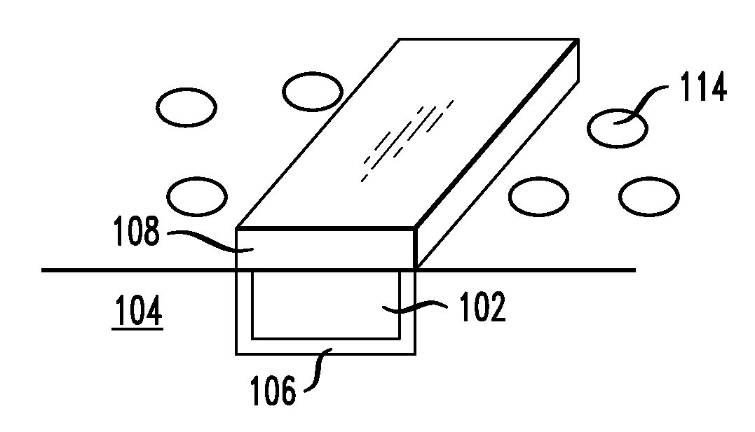
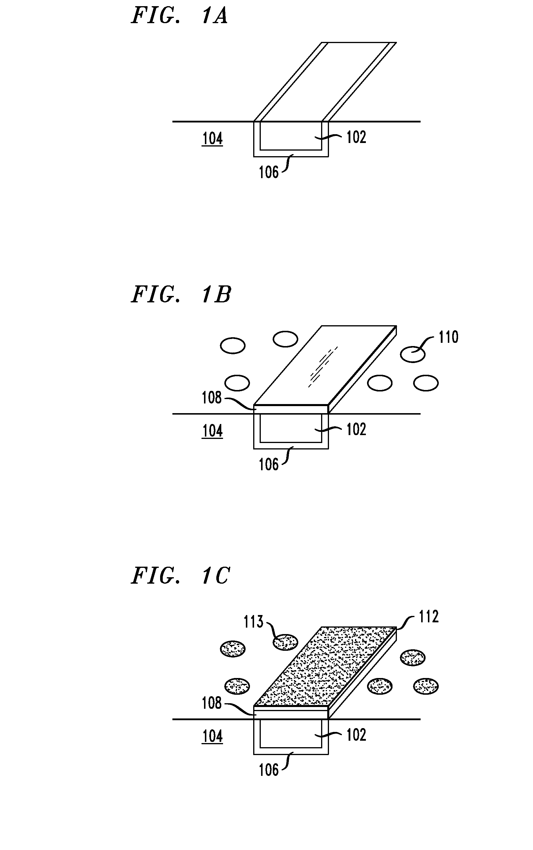
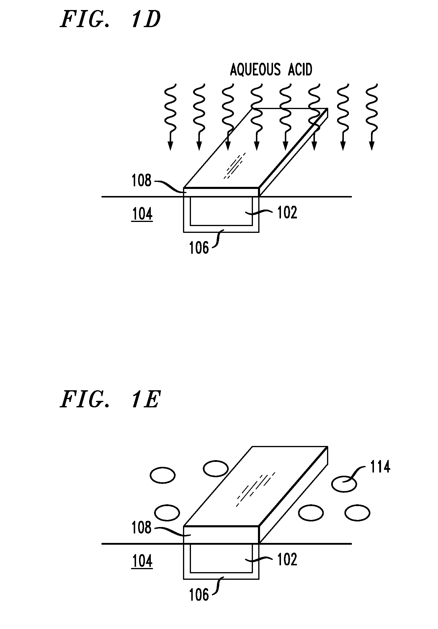
[0009]FIGS. 1A-E are cross-sectional diagrams illustrating an exemplary methodology for forming a ruthenium (Ru) capping layer on a copper (Cu) wire. As shown in FIG. 1A, Cu wire 102 is embedded in dielectric structure 104. Dielectric structure 104 preferably comprises a low-k dielectric, such as a SiCOH low-k dielectric. Diffusion barrier layer 106 is present between Cu wire 102 and dielectric structure 104. According to the present techniques, a Ru capping layer will be formed on the exposed, i.e., top, surface of Cu wire 102. As highlighted above, a capping layer is typically used to protect the wire during subsequent processing. Advantageously, the capping layers described herein (i.e., Ru capping layers over Cu wires) further serve to suppress electromigration of the Cu in the wire.

[0010]As shown in FIG. 1B, Ru layer 108 is formed on Cu wire 102. Specifically, chemical vapor deposition (CVD) of Ru is performed for a duration of which there is preferential selective nucleation o...


PUM

PropertyMeasurementUnit
thicknessaaaaaaaaaa
thicknessaaaaaaaaaa
temperatureaaaaaaaaaa

Abstract

Techniques for forming a ruthenium (Ru) capping layer on a copper (Cu) wire are provided. In one aspect, a method of forming a Ru capping layer on at least one exposed surface of a Cu wire embedded in a dielectric structure includes the following steps. A first Ru layer is selectively deposited onto the Cu wire and the dielectric structure by chemical vapor deposition (CVD) for a period of time during which selective nucleation of the Ru occurs on the surface of the Cu wire. Any nucleated Ru present on the dielectric structure is oxidized. The oxidized Ru and an aqueous acid are contacted to remove the oxidized Ru from the dielectric structure based on a selectivity of the aqueous acid in dissolving the oxidized Ru. A second Ru layer is selectively deposited onto the first Ru layer by CVD to produce a thicker Ru layer. The steps of oxidizing and contacting the oxidized Ru and an aqueous acid are repeated until a Ru layer having a thickness that is suitable for use as a Ru capping layer on at least one exposed surface of the Cu wire embedded in the dielectric structure is achieved.

Description

FIELD OF THE INVENTION [0001]The present invention relates to wiring structures and more particularly, to techniques for forming a ruthenium (Ru) capping layer over a copper (Cu) wire.BACKGROUND OF THE INVENTION [0002]Copper (Cu) wires are generally formed by first patterning a dielectric, e.g., using photolithography, with a layout of the wires. A diffusion barrier layer is deposited in the pattern. The pattern is filled with Cu to form the wires. A capping layer is then deposited over the wires, which serves to protect the wires during subsequent processing. In conventional configurations, the capping layer typically comprises a layer of dielectric over the wires.[0003]From the standpoint of electromigration, however, ruthenium (Ru) as a capping layer for Cu wires provides improved performance over the conventional dielectric capping layer. Unfortunately, one obstacle to the use of Ru as a capping layer is that during deposition of the Ru over the Cu wires, the dielectric can beco...

Claims


Application Information

Patent Timeline
Patent Type & Authority Applications(United States)
IPC IPC(8): B05D5/12
CPCC23C16/04C23C16/16C23C16/56H01L21/7685H01L21/28562H01L21/76849H01L21/02068
Inventor MCFEELY, FENTON READYANG, CHIH-CHAOYURKAS, JOHN JCOBS
Owner IBM CORP
Features
  • R&D
  • Intellectual Property
  • Life Sciences
  • Materials
  • Tech Scout
  • Unparalleled Data Quality
  • Higher Quality Content
  • 60% Fewer Hallucinations
Learn More