GaN-BASED SEMICONDUCTOR ELEMENT AND METHOD OF MANUFACTURING THE SAME

a technology semiconductor elements, which is applied in the field can solve the problems of adverse effect on inability to change the threshold value of gan-based semiconductor elements,

Inactive Publication Date: 2011-03-03
FURUKAWA ELECTRIC CO LTD
View PDF4 Cites 19 Cited by
  • Summary
  • Abstract
  • Description
  • Claims
  • Application Information

AI Technical Summary

Problems solved by technology

The inventors found that in a GaN series semiconductor element such as a GaN series MOSFET, dangling bonds in a SiO2 film that is formed by the plasma CVD method as a gate insulting film are a cause of not being able to change the threshold value of the GaN series semiconductor element according to theory.
However, it was found that in SiO2 film that is formed by the plasma CVD method, part of the Si—O bonds are broken and dangling bonds in which the Si atoms are not terminated occur, the crystal structure of the SiO2 film becomes disturbed such as Si—H bonds occurring in which H (hydrogen) terminates the Si, and in this portion positive or negative charge occurs, having an adverse effect on the threshold value of the GaN series semiconductor element.

Method used


Image

  • GaN-BASED SEMICONDUCTOR ELEMENT AND METHOD OF MANUFACTURING THE SAME
  • GaN-BASED SEMICONDUCTOR ELEMENT AND METHOD OF MANUFACTURING THE SAME
  • GaN-BASED SEMICONDUCTOR ELEMENT AND METHOD OF MANUFACTURING THE SAME

Examples


first embodiment

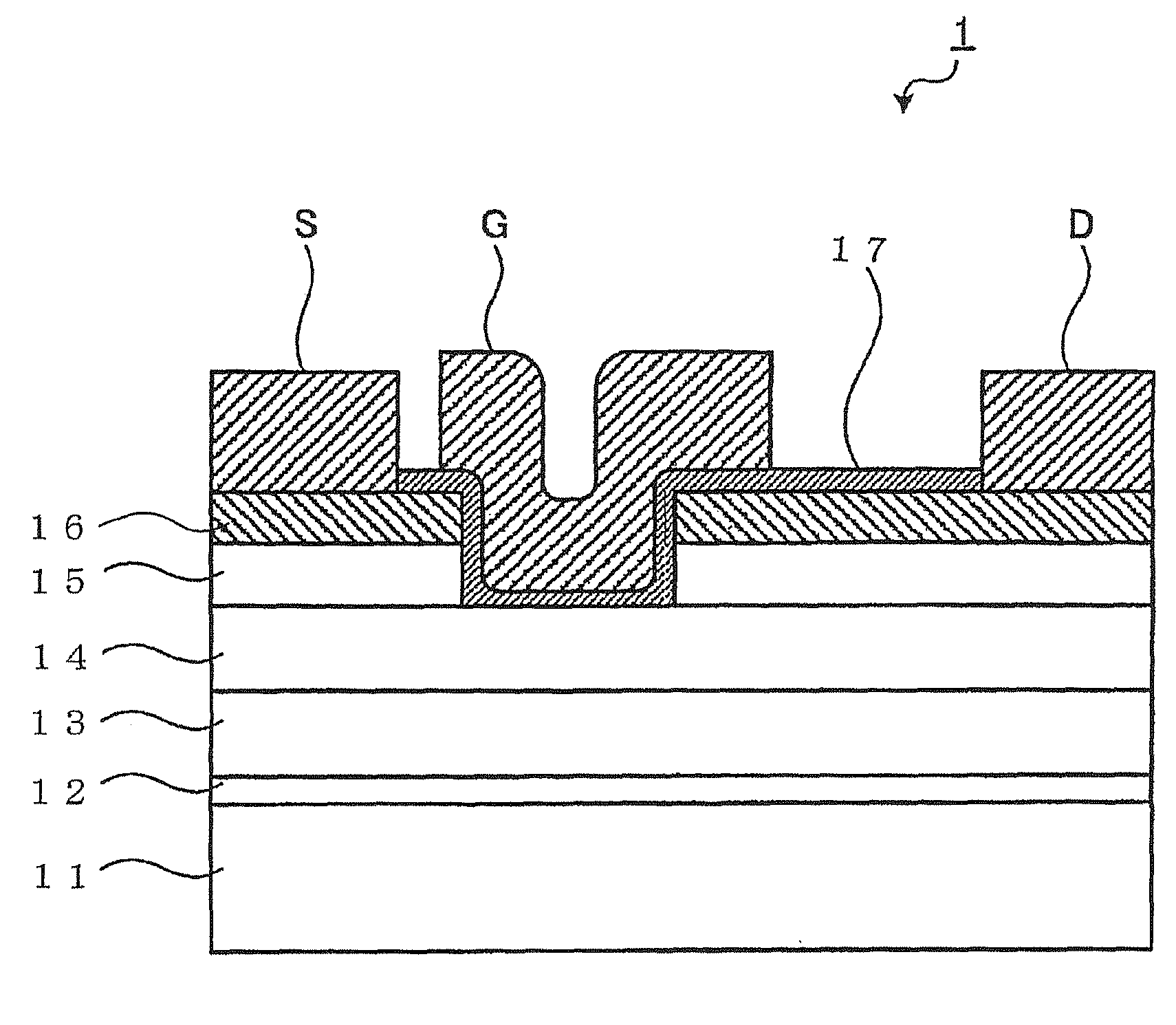
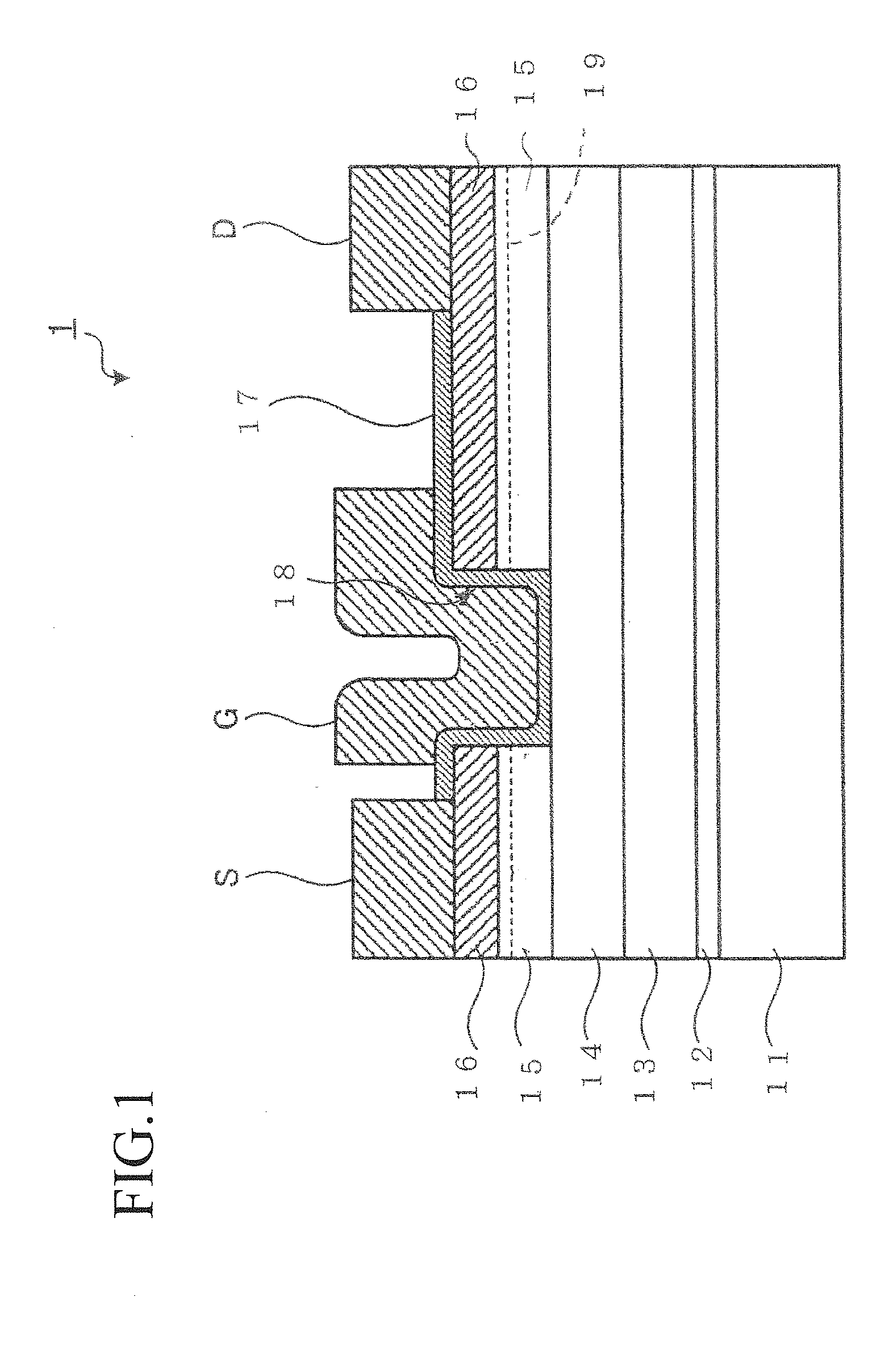
[0037]FIG. 1 is a cross-sectional drawing of the construction of a GaN series semiconductor element 1 of a first embodiment of the present invention.

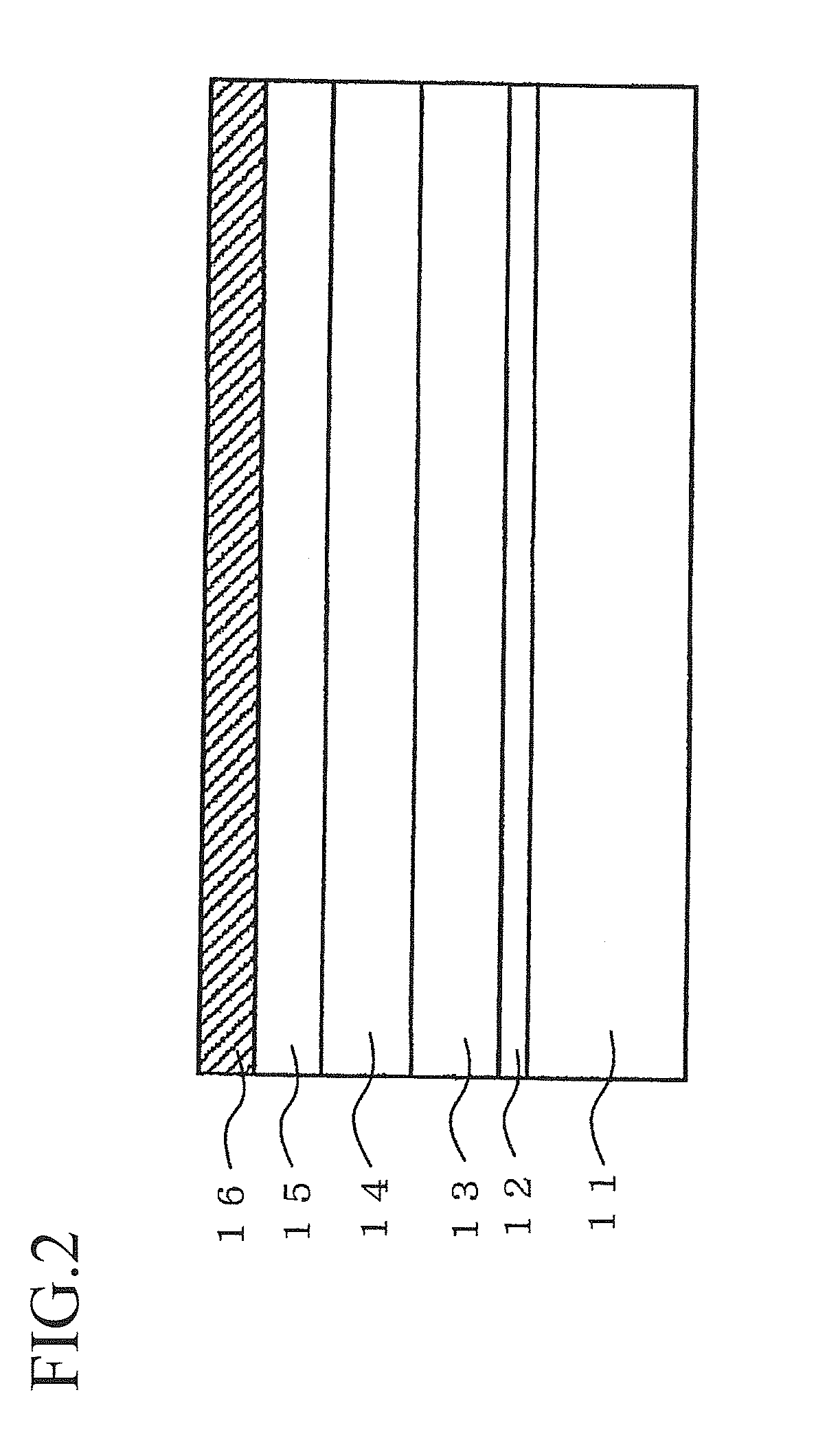
[0038]The GaN series semiconductor element 1 is a MOSFET. The GaN series semiconductor element 1 comprises an AlN layer 12, a buffer layer 13 that is formed having alternately stacked GaN layers and AlN layers, and a channel layer 14 comprising a p-GaN layer, all formed on a substrate 11 made from a material such as sapphire, SiC or Si.

[0039]An electron transit layer 15 comprising undoped GaN (un-GaN), and an electron supply layer 16 comprising a GaN series semiconductor (AlGaN) having larger bandgap energy than the electron transit layer 15 are sequentially stacked on the channel layer 14, to form an operating layer. The electron transit layer 15 and part of the electron supply layer 16 (gate electrode formation region) are removed to a depth that reaches the channel layer, to form a recess section 18.

[0040]A source electrode 21 and dr...


PUM


Abstract

Provided is a GaN series semiconductor element, which is capable of obtaining an adequate normally-off characteristic, and a manufacturing method thereof.In a GaN series semiconductor element that comprises an operating layer comprising a GaN series compound semiconductor, a gate insulating film that is formed on the operating layer, and a gate electrode that is formed on the gate insulating film, the gate insulating is a SiO2 film of which an infrared absorption peak that corresponds to the vibration energy of a Si—H bond does not appear in the absorption spectrum of transmitted light that is obtained by the Fourier transform infrared spectroscopy method. This kind of SiO2 film is a high-quality SiO2 film in which the occurrence of Si—H bonds and dangling bonds is suppressed. With this kind of construction, adverse effects on the control of the threshold value of the GaN series semiconductor element are also suppressed, so an adequate normally-off characteristic is obtained.

Description

BACKGROUND OF THE INVENTION[0001]1. Field of the Invention[0002]The present invention relates to a GaN-series semiconductor element comprising a nitride-series compound semiconductor that is used as a power-electronics device or high-frequency amplification device, and to the manufacturing method thereof.[0003]2. Description of the Related Art[0004]Wide bandgap semiconductors that are representative of group III-V nitride-series compound semiconductors have a high breakdown voltage, good electron transport properties, and good thermal conductivity, so are extremely promising as materials for semiconductor devices that are used in high-temperature environments, require high power or require high frequency. For example, in an AlGaN / GaN heterostructure, 2-dimensional electron gas is produced at a boundary face due to the piezoelectric effect. This 2-dimensional electron gas has high electron mobility and high carrier density, and has already been put into practical use in high-frequenc...

Claims


Application Information

Patent Timeline
Patent Type & Authority Applications(United States)
IPC IPC(8): H01L29/20H01L21/28
CPCH01L21/02164H01L21/02271H01L21/28264H01L21/31608H01L29/7787H01L29/2003H01L29/4236H01L29/51H01L29/66462H01L29/1083
Inventor SATO, YOSHIHIRONOMURA, TAKEHIKOKAMBAYASHI, HIROSHINAGATA, SHINJI
Owner FURUKAWA ELECTRIC CO LTD
Why Eureka
Try Eureka