Level shifter circuit

a shifter circuit and level technology, applied in the direction of pulse generators, pulse techniques, electrical apparatus, etc., can solve the problem of increasing the complexity of layout design, and achieve the effect of avoiding hot-carrier degradation and minimizing leakage curren

Inactive Publication Date: 2011-03-03
NXP BV
View PDF8 Cites 2 Cited by
  • Summary
  • Abstract
  • Description
  • Claims
  • Application Information

AI Technical Summary

Benefits of technology

[0008]It is therefore an object of the present invention to provide an improved high-voltage level shifter circuit in a simple configuration capable to avoid hot-car...

Problems solved by technology

Thereby, the complexity of t...

Method used


Image

  • Level shifter circuit
  • Level shifter circuit
  • Level shifter circuit

Examples


first embodiment

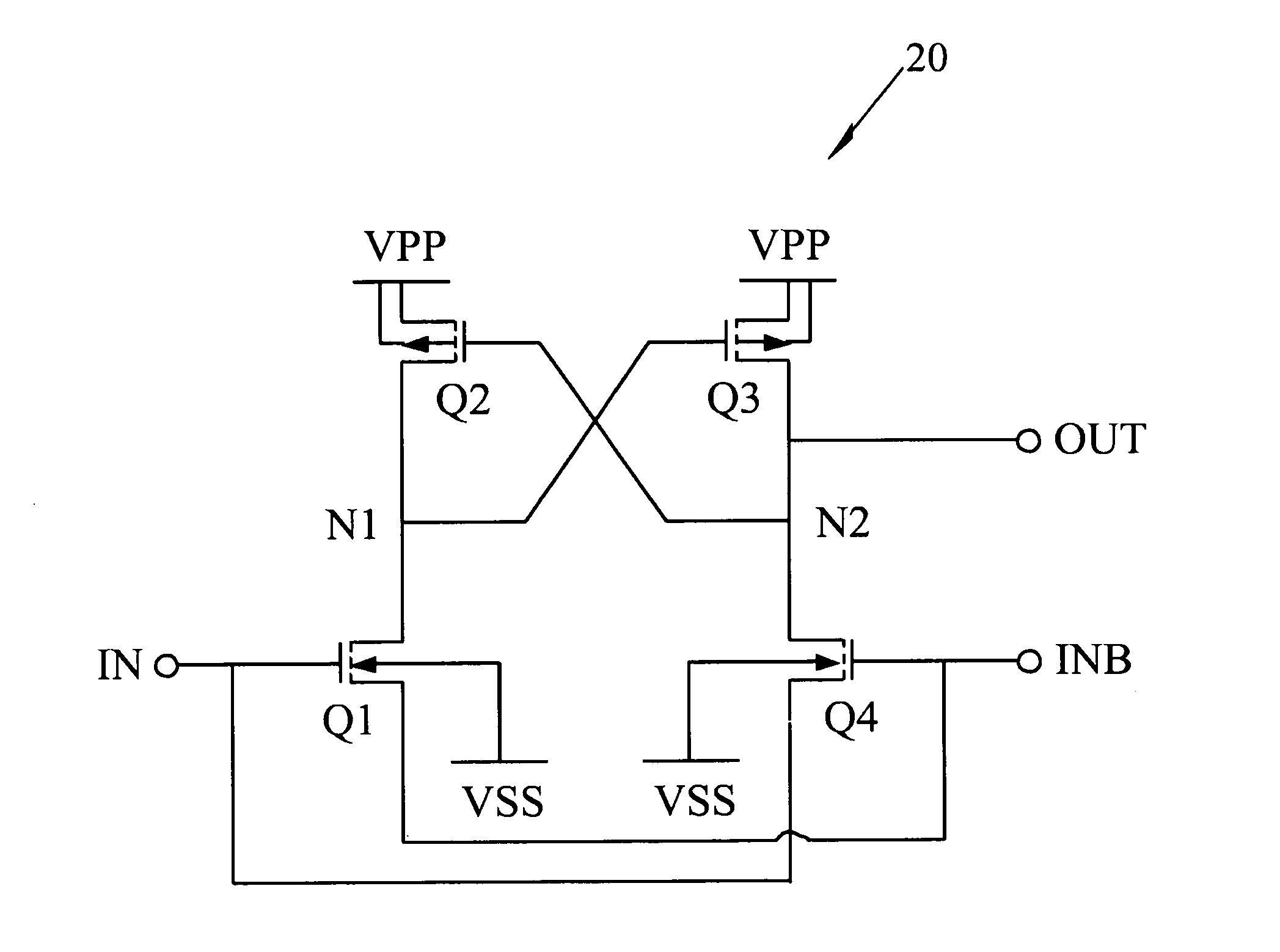
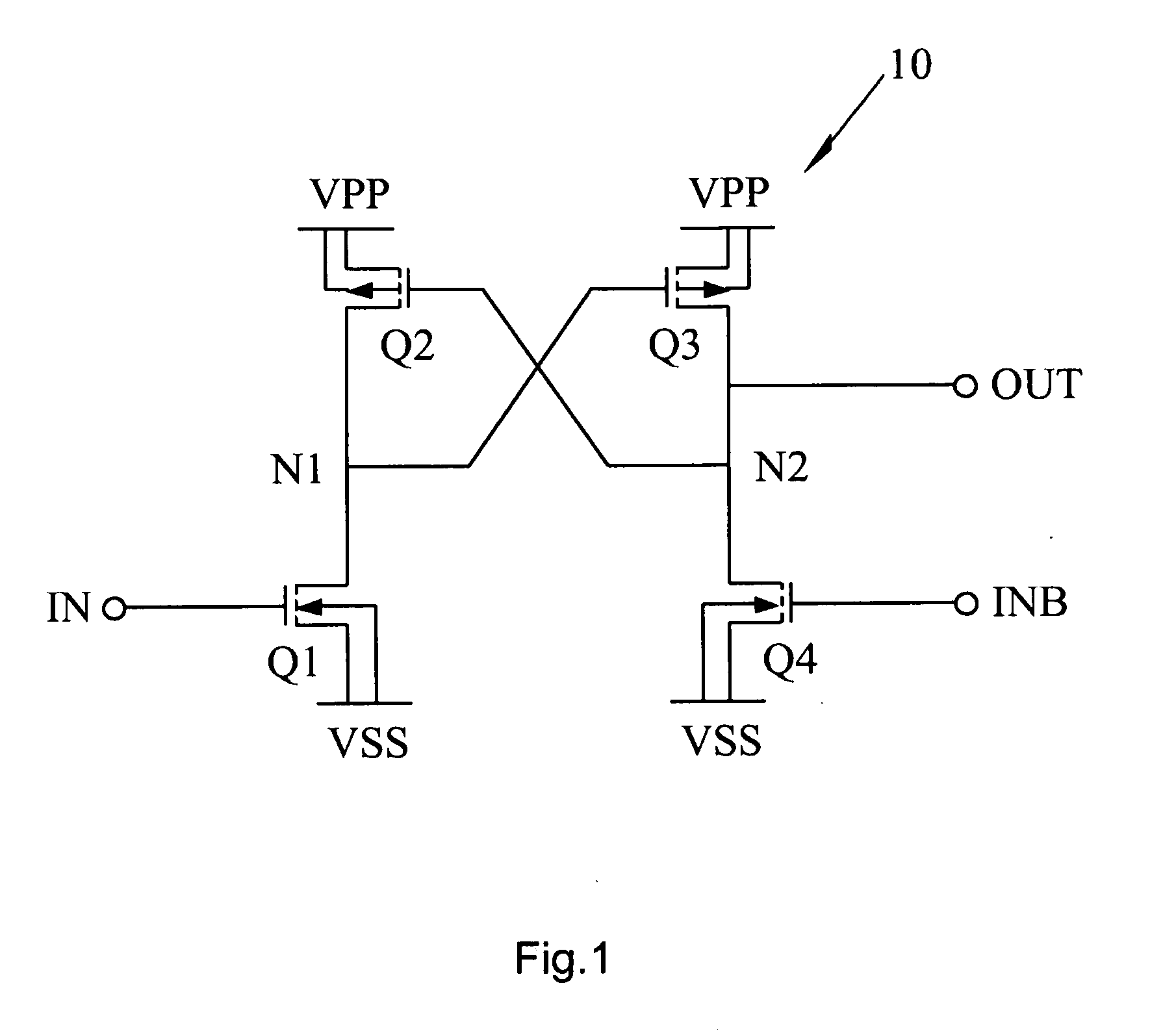
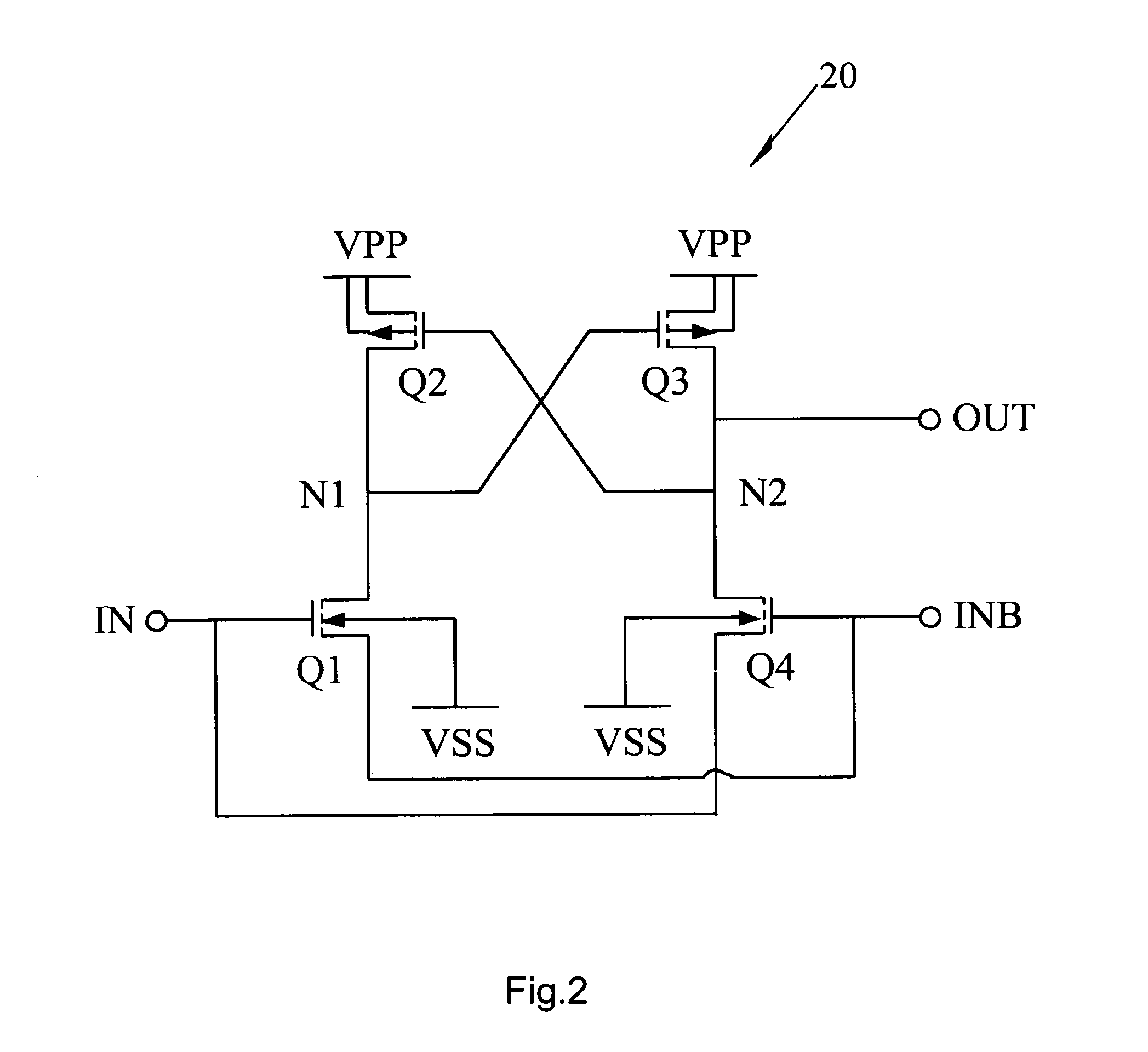
[0021]FIG. 2 is a positive 4-transistor level shifter circuit 20 according to the present invention. Such level shifter circuit 20 comprises two N-type transistors Q1 and Q4 provided at the side of a reference voltage VSS, e.g. grounded voltage, and receiving, through the use of an inverter (not shown), complementary input signals from an input terminal IN and an input terminal INB, respectively. Both inputs being supplied by a row decoder for example. Two P-type transistors Q2 and Q3 are provided at the side of a power supply voltage, e.g. programming voltage VPP, generated by an on-chip charge pump for example. The cross-coupled transistors Q2 and Q3 constitute a flip-flop wherein the gate terminal of each transistor is connected to the drain terminal of the other at a series-connection node N2 of the transistors Q3 and Q4 and at a series-connection node N1 of the transistors Q1 and Q2, respectively. The substrate and source terminal of each of them is connected to the power suppl...

second embodiment

[0025]FIG. 3 is a positive 6-transistor level shifter circuit 30 according to the present invention. Such level shifter circuit 30 comprises two N-type transistors Q1 and Q4 provided at the side of a reference voltage VSS, e.g. grounded voltage, and receiving, through the use of an inverter (not shown), complementary input signals from an input terminal IN and an input terminal INB, respectively. Both inputs are supplied by a row decoder for example. Two P-type transistors Q2 and Q3 are provided at the side of a power supply voltage, e.g. programming voltage VPP, generated by an on-chip charge pump for example, and two additional P-type transistors Q5 and Q6 coupled between the transistors Q1 and Q2 for Q5 and Q3 and Q4 for Q6. The gates of the transistors Q2 and Q3 are cross-connected to the series-connection nodes N4 of the transistors Q4 and Q6 and to the series-connection node N3 of the transistors Q1 and Q5, respectively. The substrate of the transistors Q2, Q3, Q5 and Q6 is co...


PUM


Abstract

The present invention relates to a level shifter circuit (20) for transistors requiring high voltage, such as nonvolatile memories. In the circuit configuration, the drain- to-source voltage across the NMOS transistors (Q1, Q4) can be substantially equal to the power supply voltage (VPP) according to the input voltage level at the complementary input terminals (IN, INB). For alleviating such a voltage stress, the source potential of each NMOS transistor is increased according to the input voltage level. Thus, the source of the transistor at the OUT side is biased by the input signal at the input terminal (IN) and the source of the transistor at the IN side is biased by the complementary input signal at the corresponding terminal (INB). Hot-carrier degradation and leakage of the load current flowing through from the power supply voltage (VPP) to the reference voltage (VSS) can be then reduced.

Description

FIELD OF THE INVENTION[0001]The present invention relates to the field of level shifter circuits, and more specifically to high-voltage level shifter transistors for reducing voltage stress and leakage.BACKGROUND OF THE INVENTION[0002]Level shifters have been used in many applications in which a transition from a voltage level to a higher voltage level is needed. For example, an integrated circuit may be required to drive a digital output pin with a logic one voltage level higher than the logic one voltage level used by the internal logic of the integrated circuit. In the alternative, level shifters may be used to transition from a voltage level to a lower voltage level.[0003]For applications in nonvolatile semiconductor memory transistors such as EEPROM (Electrically-Erasable Programmable Read-Only Memory), flash EEPROM, NOVRAM (Non Volatile Random Access Memory), OTP (One-Time Programmable) or MTP (Multiple-Time Programmable) nonvolatile memory, it is conventional to use level shi...

Claims


Application Information

Patent Timeline
IPC IPC(8): H03K3/356
CPCH03K3/35613
Inventor STORMS, MAURITS M. N.
Owner NXP BV
Why Eureka
Try Eureka