Semiconductor device

a technology of semiconductor devices and capacitors, applied in the direction of instruments, machines without intermediate ac conversion, process and machine control, etc., can solve the problems of reduced current driving capability, so as to prevent a reduction in current driving capability and increase the circuit area.

Inactive Publication Date: 2011-03-03
RENESAS ELECTRONICS CORP
View PDF5 Cites 11 Cited by
  • Summary
  • Abstract
  • Description
  • Claims
  • Application Information

AI Technical Summary

Benefits of technology

[0018]In the semiconductor device according to an exemplary aspect of the present invention, the current paths for collecting and discharging electric charge from the output terminal are isolated from the nodes at which the first and second control signals for controlling the drive transistors are generated. Therefore, the signal level of the first and second control signals is not affected by an increase in potential of the pumping nodes due to the electric charge pumped out of the output terminal. Consequently, in the charge pump circuit according to an exemplary aspect of the present invention, the ideal on / off state of the drive transistors can be constantly obtained, and the reduction in the current driving capability can be prevented.
[0019]The semiconductor device according to an exemplary aspect of the present invention is capable of preventing a reduction in the current driving capability without increasing the circuit area.

Problems solved by technology

The present inventor has found a problem that, in any charge pump circuit disclosed in Japanese Unexamined Patent Application Publication No. 06-150652, the current driving capability of the circuit configuration is reduced.
This causes a problem that the pumping capacitors 104 and 111 supplied with the high-level clock signal are not fully charged up.
Further, an overload state in which a large amount of electric charge is supplied to other circuits from the substrate causes a problem that the current driving capability is further reduced compared to the above-mentioned state.
This causes a problem of a further reduction in the current driving capability of the charge pump circuit 100.
This causes a problem of a reduction in the current driving capability.
Therefore, in the technique disclosed in Japanese Unexamined Patent Application Publication No. 06-150652, the driving capability is reduced due to the circuit configuration.
When the solving means is used, however, there is a problem of an increase in circuit area.

Method used


Image

  • Semiconductor device
  • Semiconductor device
  • Semiconductor device

Examples


first exemplary embodiment

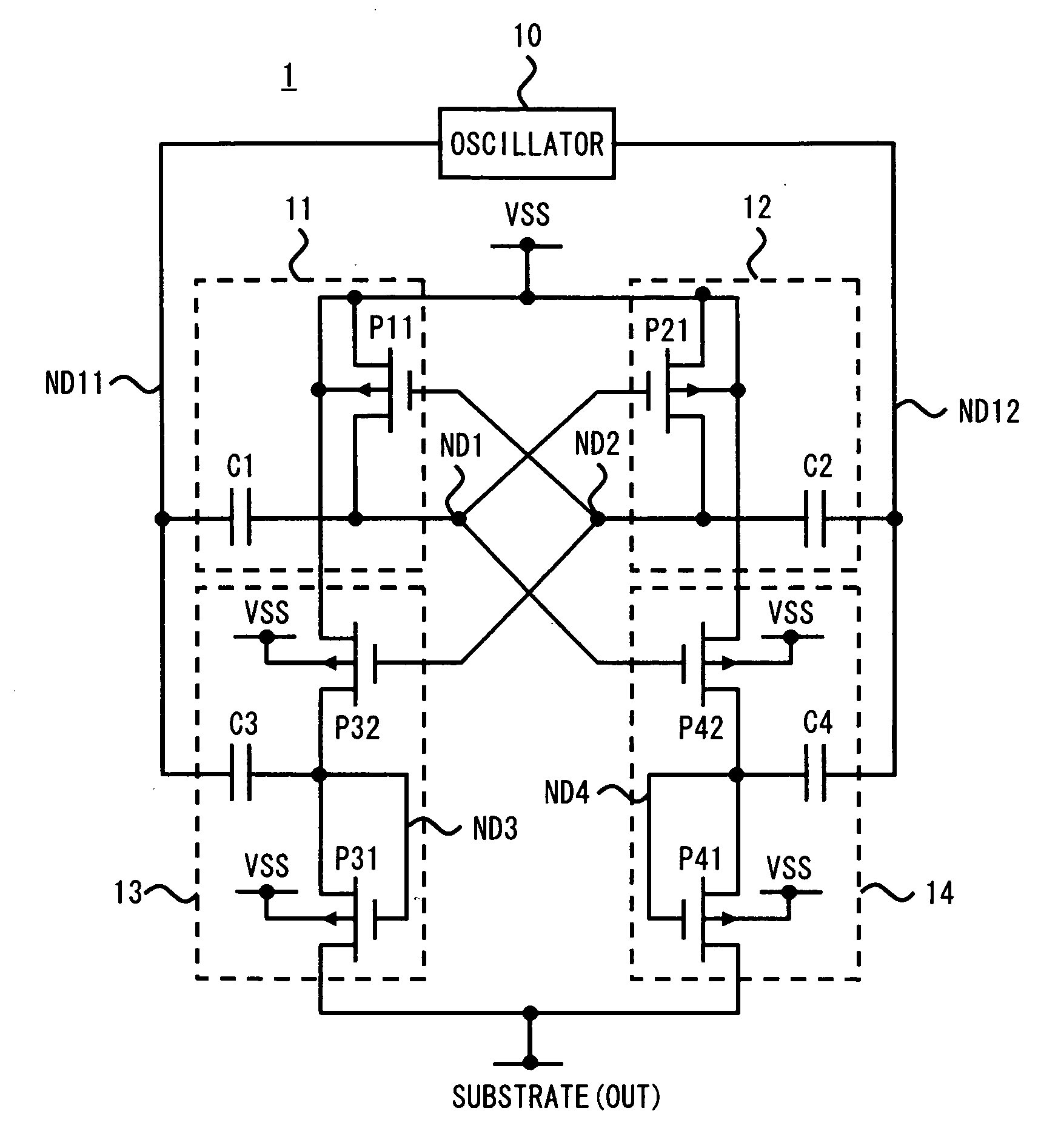
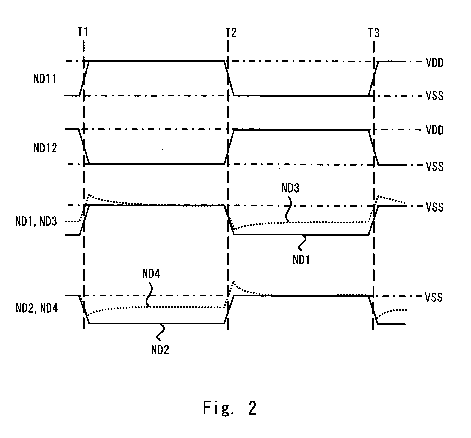
[0026]Exemplary embodiments of the present invention will be described below with reference to the accompanying drawings. FIG. 1 shows a circuit diagram of a charge pump circuit 1 provided in a semiconductor device according to a first exemplary embodiment of the present invention. As shown in FIG. 1, the charge pump circuit 1 includes an oscillator 10, a first charge pump circuit 11, a second charge pump circuit 12, a third charge pump circuit 13, and a fourth charge pump circuit 14. The charge pump circuit 1 uses a ground voltage VSS which is supplied as a reference voltage from a reference voltage terminal. Further, the charge pump circuit 1 generates a voltage for a substrate region of the semiconductor device in which the charge pump circuit is formed. That is, in the charge pump circuit 1, the substrate region of the semiconductor device corresponds to an output terminal. Assume that the charge pump circuit 1 outputs a voltage (negative voltage), which is lower than the refere...

second exemplary embodiment

[0043]FIG. 3 shows a circuit diagram of a charge pump circuit 2 according to a second exemplary embodiment of the present invention. As shown in FIG. 3, the charge pump circuit 2 has a configuration in which the first and second rectifier elements of the charge pump circuit 1 according to the first exemplary embodiment are implemented using NMOS transistors. In the charge pump circuit 2 according to the second exemplary embodiment, an NMOS transistor N31 is used as the first rectifier element, and an NMOS transistor N41 is used as the second rectifier element.

[0044]The NMOS transistor N31 has a source (terminal connected to a backgate terminal) connected to the substrate region, a drain connected to the third pumping node ND3, and a gate connected to the second pumping node ND2. That is, the conductive state of the NMOS transistor N31 is controlled by the second control signal. The NMOS transistor N41 has a source (terminal connected to a backgate terminal) connected to the substrat...

third exemplary embodiment

[Third exemplary embodiment]

[0047]FIG. 4 shows a circuit diagram of a charge pump circuit 3 according to a third exemplary embodiment of the present invention. The charge pump circuit 3 is a positive-voltage charge pump and shown as a modified example of the charge pump circuit 2. As shown in FIG. 4, the output terminal of the charge pump circuit 3 is connected not to the substrate region but to a circuit (not shown) of a power supply destination, for example. Further, a power supply terminal is used as the reference voltage terminal, and a power supply voltage VDD is supplied as the reference voltage. Furthermore, in the charge pump circuit 3, NMOS transistors are used as the first to fourth drive transistors, and PMOS transistors are used as the rectifier elements. Referring to FIG. 4, an NMOS transistor N11 is illustrated as the first drive transistor, an NMOS transistor N21 is illustrated as the second drive transistor, an NMOS transistor N32 is illustrated as the third drive tr...


PUM


Abstract

Provided is a semiconductor device including: a first charge pump circuit that generates a first control signal based on electric charge of a first pumping capacitor accumulated through a first drive transistor; a second charge pump circuit that generates a second control signal based on electric charge of a second pumping capacitor accumulated through a second drive transistor; a third charge pump circuit that transfers electric charge between an output terminal and a reference voltage terminal through a third drive transistor; and a fourth charge pump circuit that transfers electric charge between the output terminal and the reference voltage terminal through a fourth drive transistor. Conductive states of the first and third drive transistors are controlled based on the second control signal, and conductive states of the second and fourth drive transistors are controlled based on the first control signal.

Description

INCORPORATION BY REFERENCE[0001]This application is based upon and claims the benefit of priority from Japanese patent application No. 2009-196333, filed on Aug. 27, 2009, the disclosure of which is incorporated herein in its entirety by reference.BACKGROUND[0002]1. Field of the Invention[0003]The present invention relates to a semiconductor device, and more particularly, to a semiconductor device including a charge pump circuit.[0004]2. Description of Related Art[0005]Recently, in semiconductor devices, cost reduction is achieved by reducing the chip area. Meanwhile, some of the semiconductor devices include a charge pump circuit with a large circuit area as one of power supply circuits. Under this circumstance, a reduction in the area of the charge pump circuit is highly effective in reducing the cost of the semiconductor devices. However, the charge pump circuit is required to have a high current driving capability, since the charge pump circuit serves as a power supply circuit. ...

Claims


Application Information

Patent Timeline
Patent Type & Authority Applications(United States)
IPC IPC(8): G05F1/10
CPCH02M3/07
Inventor FUJITANI, KENJI
Owner RENESAS ELECTRONICS CORP
Why Eureka
Try Eureka