Supercharge Your Innovation With Domain-Expert AI Agents!

Tft-lcd array substrate and manufacturing method thereof

a technology of array substrate and liquid crystal display, which is applied in the manufacture of electrode systems, electric discharge tubes/lamps, instruments, etc., can solve the problems of disturbing the electrical field around the signal line, decreasing the manufacturing cost, and patterning processes

Active Publication Date: 2011-03-03
BEIJING BOE OPTOELECTRONCIS TECH CO LTD
View PDF3 Cites 16 Cited by
  • Summary
  • Abstract
  • Description
  • Claims
  • Application Information

AI Technical Summary

Benefits of technology

[0022]However, similarly to the FFS type TFT-LCD array substrate, the passivation layer in the conventional TN type TFT-LCD array substrate also has a uniform thickness in the regions corresponding to the pixel electrode, the gate line and the data line for each pixel region. As for the conventional TN type array substrate, the overlapping portion of the pixel electrode and the common electrode line is formed into a storage capacitor, forming a structure of storage on common. The thicker the passivation layer between the pixel electrode and the common electrode line, the smaller the storage capacitance.

Problems solved by technology

Therefore, the complexity of a method for manufacturing a TFT-LCD array substrate can be evaluated based on the numbers of the employed patterning processes, and reducing patterning processes means decreasing manufacturing cost.
When the liquid crystal is driven in a TFT-LCD, disturbing electrical fields is formed around the signal lines.
Among these disturbing electrical fields, the electrical filed between the common electrode above the pixel electrode and a signal line is the most harmful.
The electrical field lines of the electrical field will disturb the rotation of the liquid crystal molecules above the pixel electrode (belonging to the liquid crystal molecules used for normal displaying) so that the image cannot be displayed correctly.
However, for the array substrate of the FFS type liquid crystal display manufactured by the above four-patterning method, since there is the common electrode above the signal lines, electrical field will be generated between the signal lines and the common electrode thereabove, so that electrical field lines are concentrated in the regions above the signal lines, and the electromagnetic effect between the signal lines and the common electrode above the pixel electrode is weakened.
But, if the distance between the signal lines and the common electrode is too small, that is to say, the thickness between the signal lines and the common electrode is too thin, the electrical field formed between the common electrode and the signal lines will disturb the signals from the signal lines, which leads to signal delay and affects the display quality disadvantageously.
Especially for the liquid crystal display used in the notebook computer, the low power consumption attracts much attention.
However, for the FFS type TFT-LCD array substrate with a high aspect ratio, although the aspect ratio is increased, the too thick passivation layer leads to a large distance between the common electrode and the pixel electrode, thus, a higher driving voltage is needed for a normal operation and the power consumption is increased notably.

Method used


Image

  • Tft-lcd array substrate and manufacturing method thereof
  • Tft-lcd array substrate and manufacturing method thereof
  • Tft-lcd array substrate and manufacturing method thereof

Examples


Embodiment Construction

[0039]Hereinafter, the embodiments of the invention will be described in detail in connection with the accompanying drawings.

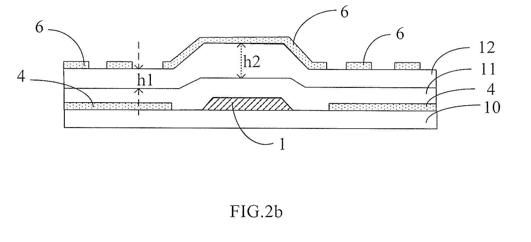
[0040]FIG. 1 is a schematic plan view of an FFS type TFT-LCD array substrate according to an embodiment of the invention. FIG. 2a is a cross-sectional view of FIG. 1 taken along line A-A, and FIG. 2b is a cross-sectional view of FIG. 1 taken along line B-B.

[0041]As shown in FIGS. 1, 2a and 2b, the FFS type TFT-LCD array substrate according to the embodiment of the invention mainly comprises a transparent substrate 10, a gate line 1, a gate insulating layer 11, a data line 2, a thin film transistor (TFT) 3, a pixel electrode 4, a common electrode line 5, a common electrode 6, a passivation layer 12 and etc. Specifically, the gate line 1 and the common electrode line 5 are provided transversely on the transparent substrate 10, and the gate insulating layer 11 covers the gate line 1 and the common electrode line 5. The data line 2 is provided on the gate insulati...


PUM


Abstract

A TFT-LCD array substrate comprising a transparent substrate and a gate line, a data line, a thin film transistor, a pixel electrode and a passivation layer that are formed on the transparent substrate. The passivation layer includes a first region corresponding to the pixel electrode, a second region corresponding to the gate line and a third region corresponding to the data line, the first region has a first thickness, the second region has the second thickness, and the third region has the third region. The first thickness is smaller than the second thickness, the second thickness is smaller or equal to the third thickness.

Description

BACKGROUND OF THE INVENTION[0001]Embodiments of the invention relate to a liquid crystal display array substrate and a manufacturing method thereof.[0002]Thin film transistor liquid crystal displays (TFT-LCDs) are an important type of flat panel displays (FPDs).[0003]TFT-LCDs can be classified into a vertical electrical field type and a horizontal electrical field type depending on the direction of the electrical field by which the liquid crystal is driven. For a vertical electrical field type TFT-LCD, a pixel electrode is formed on an array substrate while a common electrode is formed on a color filter substrate. For a horizontal electrical field type TFT-LCD, both a pixel electrode and a common electrode are formed on an array substrate. Therefore, an additional patterning process for forming the common electrode is required when a horizontal electrical filed type TFT-LCD array substrate is manufactured. A vertical electrical field type TFT-LCD comprises a twist nematic (TN) type ...

Claims


Application Information

Patent Timeline
Patent Type & Authority Applications(United States)
IPC IPC(8): G09G3/36G06F3/038H01J9/00
CPCG02F1/134363G02F1/136286G02F2001/134318H01L27/1248G02F2001/134372H01L27/1255G02F2001/13606G02F1/134318G02F1/13606
Inventor CHOI, HYUN SIC
Owner BEIJING BOE OPTOELECTRONCIS TECH CO LTD
Features
  • R&D
  • Intellectual Property
  • Life Sciences
  • Materials
  • Tech Scout
  • Unparalleled Data Quality
  • Higher Quality Content
  • 60% Fewer Hallucinations
Learn More