

Porous amorphous silicon-carbon nanotube composite based electrodes for battery applications
- Summary
- Abstract
- Description
- Claims
- Application Information
AI Technical Summary
Benefits of technology
Problems solved by technology
Method used
Image

Examples
examples
[0101]The following hypothetical non-limiting examples are provided to further illustrate embodiments described herein. However, the examples are not intended to be all inclusive and are not intended to limit the scope of the embodiments described herein.
Porous Si-CNT on a 300 mm Substrate:
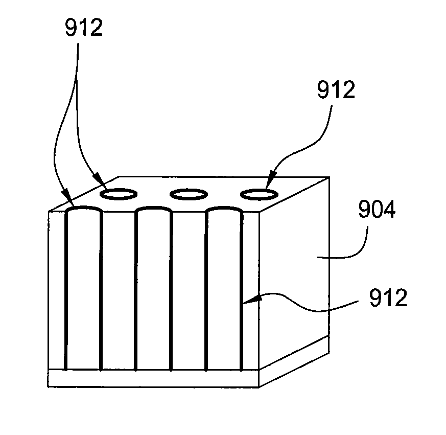
[0102]With reference to FIG. 11 and FIGS. 9A-9D, the substrate S is transferred into the integrated processing tool 1100. The substrate is transferred into the first PVD chamber 1112 where copper is deposited on the substrate S using a PVD sputtering process. The substrate S is transferred to the second PVD chamber 1114 where the silicon (Si) matrix 904 with an aluminum (Al) phase 906 segregated therein is deposited on the substrate S as shown in FIG. 9B. Next, the substrate S is transferred to a wet etch chamber where the aluminum phase 906 is removed from the silicon matrix 904 using a wet etch process. The wet etch may be performed either in a dedicated wet etch chamber coupled with the integra...
PUM
| Property | Measurement | Unit |
|---|---|---|
| Temperature | aaaaa | aaaaa |
| Diameter | aaaaa | aaaaa |
| Diameter | aaaaa | aaaaa |
Abstract
Description
Claims
Application Information