Nano-wire field effect transistor, method for manufacturing the transistor, and integrated circuit including the transistor

a technology of nanowire field and transistor, which is applied in the direction of nanotechnology, electrical apparatus, semiconductor devices, etc., can solve the problems of less than 1% of inefficient power consumption due to leakage current rather than operating power increase, difficult to perfectly suppress leakage current increase and sub-threshold slope, and improve the variation in size and characteristics. , the effect of superior size reproducibility and uniformity

Inactive Publication Date: 2011-03-10
NAT INST OF ADVANCED IND SCI & TECH
View PDF5 Cites 63 Cited by
  • Summary
  • Abstract
  • Description
  • Claims
  • Application Information

AI Technical Summary

Benefits of technology

[0024]In accordance with the present invention, there are provided two nano-wires arranged one above the other on an SOI substrate having a (100) surface orientation. Therefore, the driving current of the transistor becomes twice as large as that of the conventional nano-wire field effect transistor with the same device area.
[0025]In addition, by fabricating the nano-wire with orientation dependent wet etching, the channel has a smooth surface with an atomic layer order which is superior in size reproducibility and uniformity.
[0026]Therefore, the present invention can improve a variation in size and characteristics in the conventional nano-wire having a circular cross-section shape formed by high temperature hydrogen annealing or thermal oxidizing from a nonuniform silicon thin wire prepared by RIE (Reactive Ion Etching).

Problems solved by technology

However, it is deeply concerned that miniaturization of the conventional bulk type CMOS integrated circuit will reach its limit in near future.
In other word, a serious problem lies in that the more the technology node progresses, the more percentage of inefficient power consumption due to the leakage current rather than the operating power increases.
Even with this double gate MOSFET, however, it is still not easy to perfectly suppress increase of the leakage current and the sub-threshold slope due to the short channel effect when the gate length of the device is decreased to 20 nm or below (corresponding to a stage after the 32 nm node).
Furthermore, the dimension of the channel is required to be small corresponding to shortening the gate length, but forming the small channel is difficult.
Since the threshold voltage of the FinFET described above is a fixed value, it is not available for applications such as dynamic electric power control.
When the threshold voltage is controlled by a gate voltage on one side, however, the sub-threshold slope inevitably increases significantly from the ideal value S=60 mV / decade, which leads to a degradation of the switching characteristics of the device.
Further problem is that the drain current decreases significantly when the threshold voltage is controlled by applying a voltage to one of the gate electrodes, since the gate bias works to a direction for one of the channels to close.
This structure, however, would enlarge the device area.

Method used


Image

  • Nano-wire field effect transistor, method for manufacturing the transistor, and integrated circuit including the transistor
  • Nano-wire field effect transistor, method for manufacturing the transistor, and integrated circuit including the transistor
  • Nano-wire field effect transistor, method for manufacturing the transistor, and integrated circuit including the transistor

Examples


first embodiment

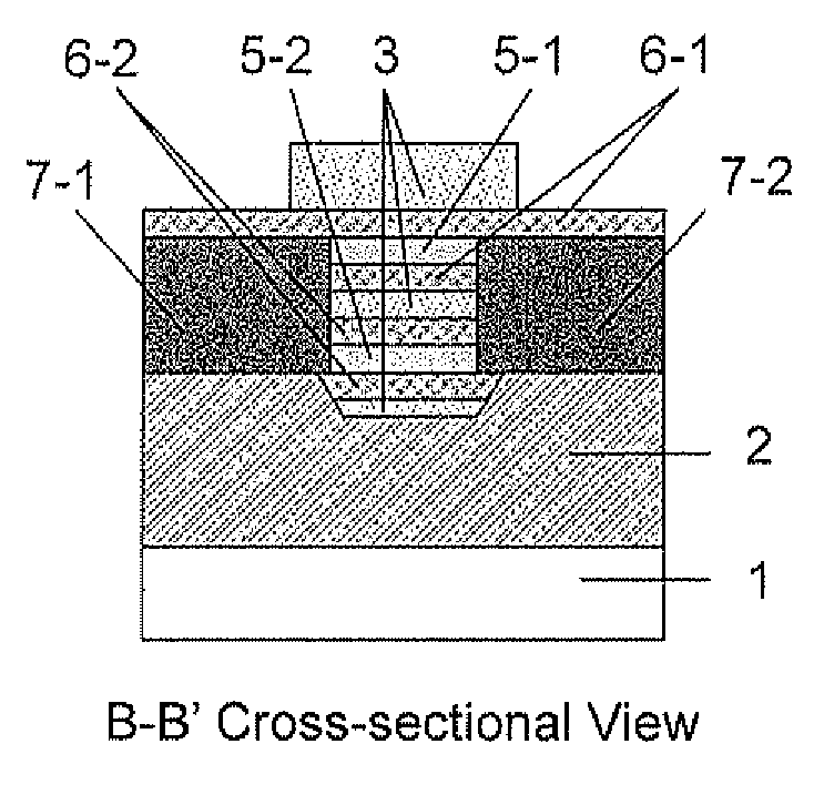
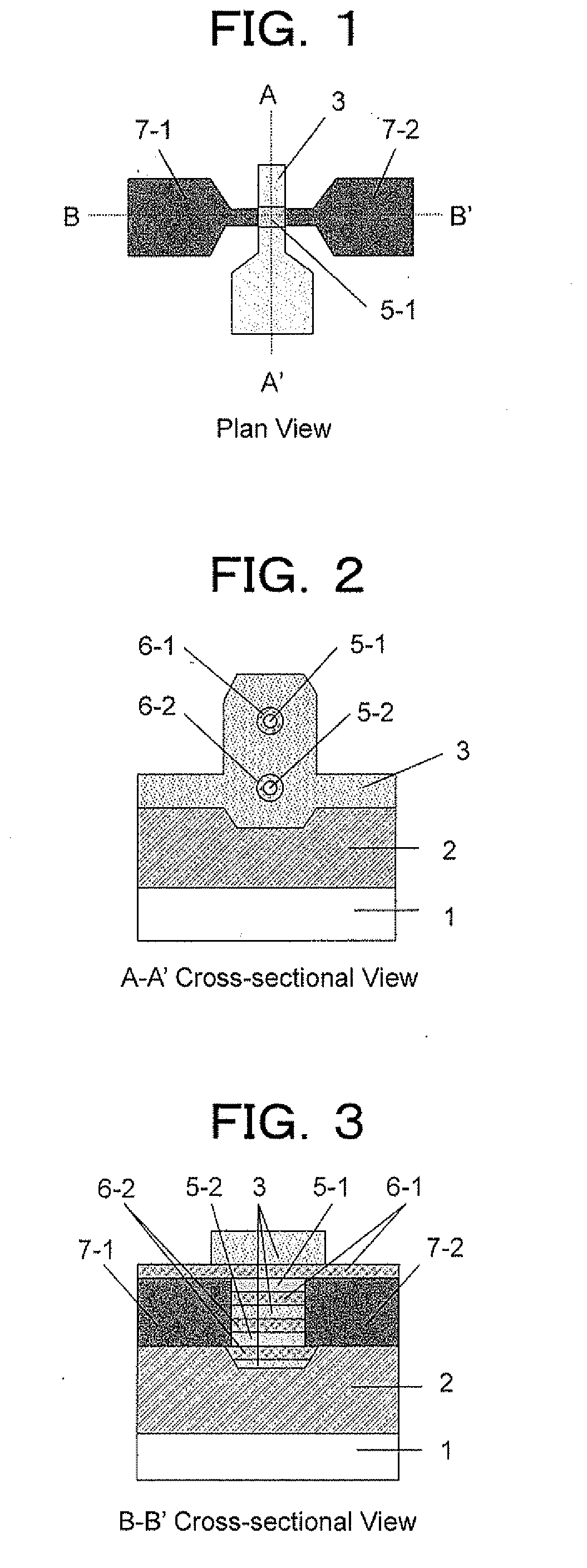
[0063]FIGS. 1, 2 and 3 show a first embodiment in accordance with the present invention. FIG. 1 is a plan view of a nano-wire field effect transistor in accordance with the present invention, the transistor having a pair of nano-wires each having a circular cross-section shape and being arranged one above the other formed on a (100) SOI substrate. FIG. 2 is an A-A′ cross-sectional view thereof, and FIG. 3 is a B-B′ cross-sectional view thereof. In FIGS. 1 to 3, numeral reference 1 denotes a substrate, 2 denotes a buried oxide film, 3 denotes a gate electrode, 5-1 and 5-2 denote nano-wares each having a circular cross-section shape and simultaneously formed one above the other. 6-1 and 6-2 are gate insulator films, and 7-1 and 7-2 are a source region and a drain region, respectively.

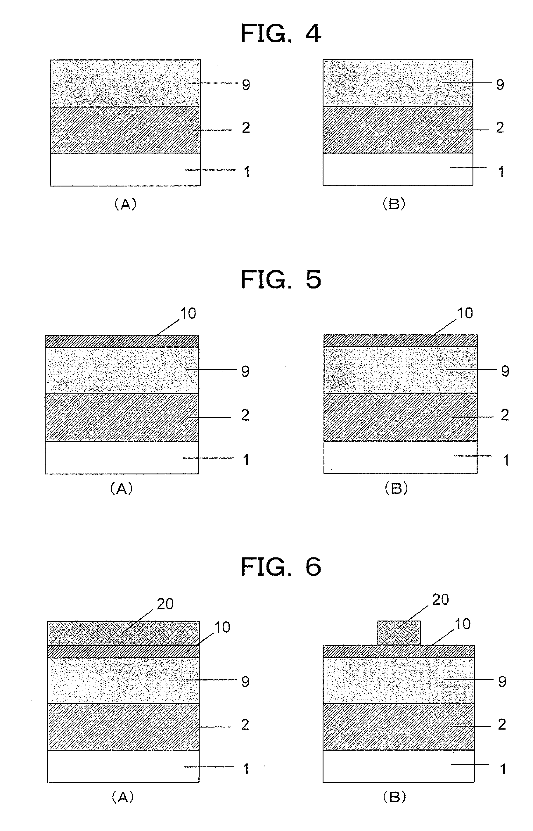
[0064]FIGS. 4 to 19 show an example of a fabrication process of the nano-wire field effect transistor having a pair of nano-wires each having a circular cross-section shape and being arranged one above th...

second embodiment

[0074]FIGS. 20, 21 and 22 show the second embodiment of the present invention. FIG. 20 shows a plan view of a nano-wire field effect transistor in accordance with the present invention. In this figure, a plurality of pairs of nano-wires each having a circular cross-section shape arranged one above the other are arranged in parallel. FIG. 21 shows an A-A′ cross-sectional view thereof, and FIG. 22 shows a B-B′ cross-sectional view thereof. In FIGS. 20 to 22, numeral reference 1 denotes a substrate, 2 denotes a buried oxide film, 3 denotes a gate electrode, 5-5, 5-6, 5-7, 5-8, 5-9, and 5-10 denote nano-wires each having a circular cross-section shape, 6-5, 6-6, 6-7, 6-8, 6-9, and 6-10 denote gate insulator films, and 7-1 and 7-2 denote source-drain regions.

[0075]A fabrication process of the second embodiment is basically same as that of the first embodiment. A different point is that in the electron beam lithography process in the above paragraph 0016, a pattern of the nano-wire is for...

third embodiment

[0076]FIGS. 23, 24, and 25 show the third embodiment of the present invention. FIG. 23 shows a plan view of an integrated circuit in accordance with the present invention. In this figure, a nano-wire field effect transistor including a pair of nano-wires each having a circular cross-section shape arranged one above the other is used as a PMOS, whereas a nano-wire field effect transistor with a nano-wire having a circular cross-section shape where the upper nano-wire a circular cross-section shape is removed by an etching is used as an NMOS. FIG. 24 shows an A1-A1′ and A2-A2′ cross-sectional views thereof, and FIG. 25 shows a B-B′ cross-sectional view thereof.

[0077]In FIGS. 23 to 25, numeral reference 1 denotes a substrate, 2 denotes a buried oxide film, 3 denotes a gate electrode, 5-1, 5-2, and 5-4 are nano-wires each having a circular cross-section shape, 6-1, 6-2, 6-3, and 6-4 denote gate insulator films, and 7-1, 7-2, 7-3, and 7-4 denote source-drain regions.

[0078]A fabrication p...


PUM


Abstract

Provided is a method for fabricating a nano-wire field effect transistor including steps of: preparing a nano-wire field effect transistor including two columnar members made of a silicon crystal configuring a nano-wire on a substrate are arranged on a substrate in parallel and one above the other, and an SOI substrate having a (100) surface orientation; processing a silicon crystal layer configuring the SOI substrate into a standing plate-shaped member having a rectangular cross-section; processing the silicon crystal by orientation dependent wet etching and thermal oxidation into a shape where two triangular columnar members are arranged one above the other with a spacing from each other as to face along the ridge lines of the triangular columnar members; and processing the triangular columnar member into a circular columnar member configuring a nano-wire by hydrogen-annealing or a thermal oxidation; and an integrated circuit including the transistor.

Description

TECHNICAL FIELD[0001]The present invention relates a nano-wire field effect transistor, a method for manufacturing the transistor, and an integrated circuit including the transistor.BACKGROUND ART[0002]Silicon integrated circuits have been progressed in enlarging the scale as well as in improving the performance according to so-called Moore's rule, and supported the development of the advanced information technology (IT) society from an aspect of the hardware. This trend is expected to be continued also in future. However, it is deeply concerned that miniaturization of the conventional bulk type CMOS integrated circuit will reach its limit in near future. Its main reasons are an increase in leakage current due to the miniaturization of the transistor, a degradation in switching property of the transistor (an increase in the sub-threshold slope) and so on. In other word, a serious problem lies in that the more the technology node progresses, the more percentage of inefficient power c...

Claims


Application Information

Patent Timeline
Patent Type & Authority Applications(United States)
IPC IPC(8): H01L29/66H01L21/762H01L29/775B82Y99/00
CPCB82Y10/00H01L29/0665H01L29/0673H01L29/78696H01L29/42392H01L29/775H01L29/125
Inventor LIU, YONGXUNMATSUKAWA, TAKASHIENDO, KAZUHIKOOUCHI, SHINICHISAKAMOTO, KUNIHIROMASAHARA, MEISHOKU
Owner NAT INST OF ADVANCED IND SCI & TECH
Why Eureka
Try Eureka