

Nano-wire field effect transistor, method for manufacturing the transistor, and integrated circuit including the transistor
a technology of nanowire field and transistor, which is applied in the direction of nanotechnology, electrical apparatus, semiconductor devices, etc., can solve the problems of increasing the percentage of ineffective power consumption due to leakage current rather than operating power, the inability to micro-manufacture the fin channel, and the inability to meet the requirements of micro-structure, etc., to achieve the effect of improving the size variation and superior size reproducibility and uniformity
- Summary
- Abstract
- Description
- Claims
- Application Information
AI Technical Summary
Benefits of technology
Problems solved by technology
Method used
Image

Examples
first embodiment
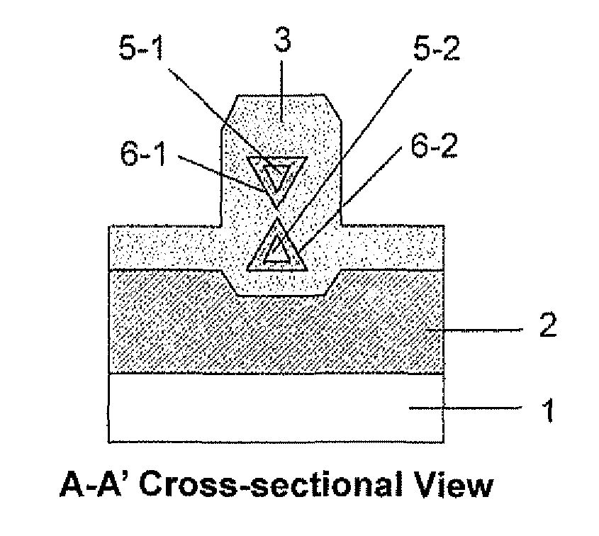
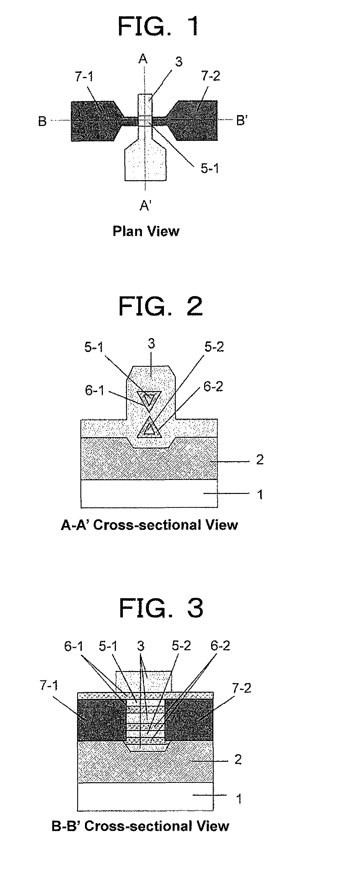
[0073]FIGS. 1, 2 and 3 show the first embodiment in accordance with the present invention. FIG. 1 is a plan view of a nano-wire field effect transistor in accordance with the present invention, having two triangular columnar members configuring the nano-wires formed on a (100) SOI substrate. FIG. 2 is an A-A′ cross-sectional view thereof, and FIG. 3 is a B-B′ cross-sectional view thereof. In FIGS. 1 to 3, numeral reference 1 denotes a substrate, 2 denotes a buried oxide film, 3 denotes a gate electrode, 5-1 and 5-2 denote nano-wires each having a triangular cross-section simultaneously formed in a vertical direction. 6-1 and 6-2 denote gate insulator film, and 7-1 and 7-2 denote a source region and a drain region, respectively.
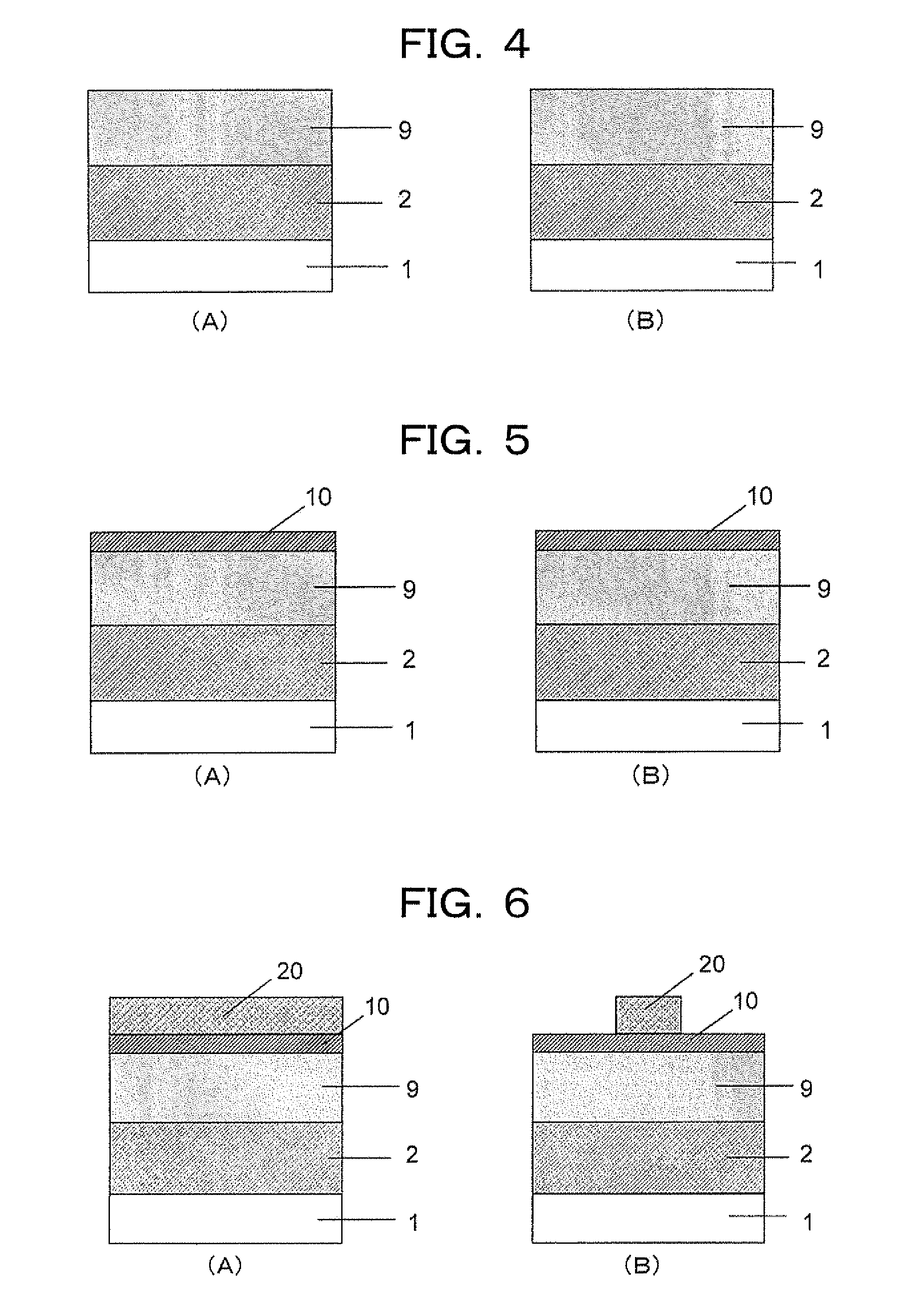
[0074]FIGS. 4 to 18 show an example of a fabrication process of the nano-wire field effect transistor in accordance with the first embodiment of the present invention. In FIGS. 4 to 18, Figure (A) shows an A-A′ cross-sectional view, and Figure (B) shows a B-B′...
second embodiment
[0083]FIGS. 19, 20 and 21 show the second embodiment of the present invention. FIG. 19 shows a plan view of a nano-wire field effect transistor in accordance with the present invention, where a plurality of pairs of triangular columnar members configuring the nano-wires are arranged in parallel. FIG. 20 shows an A-A′ cross-sectional view thereof, and FIG. 21 shows a B-B′ cross-sectional view thereof. In FIGS. 19 to 21, 1 denotes a substrate, 2 denotes a buried oxide film, 3 denotes a gate electrode, 5-3, 5-4, 5-5, 5-6, 5-7, and 5-8 denote nano-wires each having a triangular cross-section, 6-3, 6-4, 6-5, 6-6, 6-7, and 6-8 denote gate insulator films, and 7-1 and 7-2 denote source-drain regions.
[0084]A fabrication process of the second embodiment is basically the same as that of the first embodiment. A different point is that in the electron beam lithography process in the above paragraph 0018, a pattern of the nano-wire is formed in such a way that a plurality of pairs of nano-wires ...
third embodiment
[0085]FIGS. 22, 23 and 24 show the third embodiment of the present invention. FIG. 22 shows a plan view of a nano-wire field effect transistor in accordance with the present invention independent gates are provided via a gate insulating film on both side surfaces of triangular columnar members. FIG. 23 shows an A-A′ cross-sectional view thereof, and FIG. 24 shows a B-B′ cross-sectional view thereof.
[0086]In FIGS. 22 to 24, 1 denotes a substrate, 2 denotes a buried oxide film, 3-1 and 3-2 denote gate electrodes, 5-11 and 5-12 denote nano-wires each having a triangular cross-section, 6-11 and 6-12 denote gate insulator films, and 7-1 and 7-2 denote source-drain regions.
[0087]A fabrication process of the third embodiment is basically the same as that of the first embodiment, but the following two points.
[0088](1) First, during electron beam lithography of the above paragraph 0018, the width W of the resist mask 21 is precisely controlled according to the thickness H of the SOI layer, t...
PUM
 Abstract
Description
Claims
Application Information