Semiconductor memory device

Inactive Publication Date: 2011-03-10
HITACHI LTD
View PDF6 Cites 8 Cited by
  • Summary
  • Abstract
  • Description
  • Claims
  • Application Information

AI Technical Summary

Benefits of technology

In embodiments, read or write operations in the non-volatile memory array are accomplished by applying appropriate voltages for the read/write operation to a selected source line and a selected drain line. A gate voltage for the read/write operation is then applied to the gate line. The desired operation can then be performed on the memory cell connected to the se

Problems solved by technology

However, as the size of the transistor is reduced, the distance between the source 906 and the drain 904 is decreased, thereby resulting in an increase in leakage current in the transistor.
Thus, the information stored in a selected memory cell cannot be read out.
For single transistors, tuning of the impurity profile in the semiconductor substrate

Method used


Image

  • Semiconductor memory device
  • Semiconductor memory device
  • Semiconductor memory device

Examples


Example

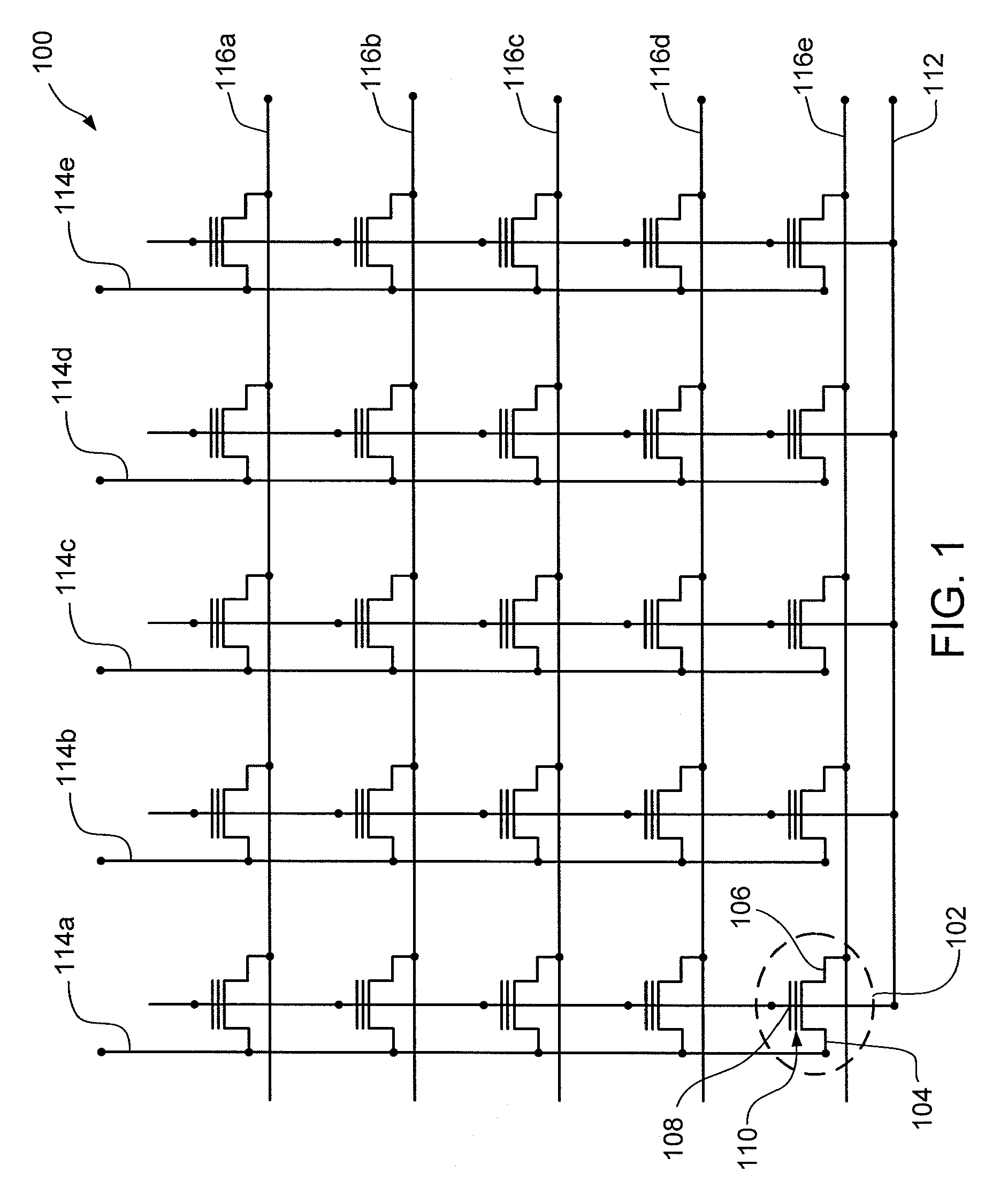
FIGS. 6A-16B show a fabrication process for the non-volatile memory cell array according to a first embodiment of the present invention. The “A” figures illustrate plan views of a step in the fabrication process. In the figures, not all layers are shown for clarity in illustration and description of the underlying features. The “B” figures illustrate cross-sectional views along line B-B in the corresponding figure “A”. In the figures, not all layers have been shown in plan view for clarity.

Referring initially to FIGS. 6A-6B, ion implantation is performed on a semiconductor substrate 602, such as a silicon wafer, to form wells therein. After the implantation, a layer of silicon nitride 604 is deposited on the substrate 602 and patterned. The patterning of the silicon nitride 604 is achieved using photolithography and etching, for example.

Referring to FIGS. 7A-7B, a cut mask 606 is formed over the patterned silicon nitride layer 604 to define active regions. With the use of the cut ma...

Example

FIGS. 17A-22B show a fabrication process for the non-volatile memory cell array according to a second embodiment of the present invention. The “A” figures illustrate plan views of a step in the fabrication process. In the figures, not all layers are shown for clarity in illustration and description of the underlying features. The “B” figures illustrate cross-sectional views along line B-B in the corresponding figure “A”. In the figures, not all layers have been shown in plan view for clarity.

The circuit diagram of the non-volatile memory array according to the second embodiment is the same as in the first embodiment (i.e., FIG. 1). Moreover, the fabrication process is similar to that of the first embodiment but has been altered to form the gate electrode and the charge storage layer using a side-wall self-alignment process.

The fabrication steps of the first embodiment prior to the patterning of the charge storage layer (e.g., FIGS. 6A-10B) are applicable to the second embodiment. Ho...

Example

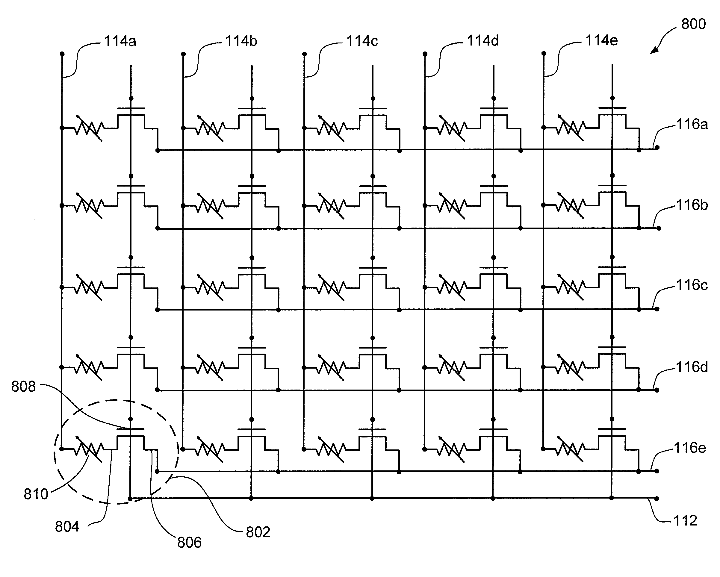
FIG. 23 is a schematic of a non-volatile memory cell array according to the third embodiment of the present invention.

In the third embodiment, the array 800 is similar to that of the first and second embodiments, as shown in FIG. 1. However, the individual memory cells 802 are different than that of the first and second embodiments. In particular, the memory cell 802 includes a transistor with a source 806, a drain 804, and a gate 808. The memory cell 802 also includes a variable resistance element 810 for storing information. For example, the variable resistance element 810 is a phase change material that stores information based on the change of resistance due to a change in phase of the material.

A plurality of source lines 116a-116e connects respective sources 806 of individual memory cells 802 in a row direction. A common gate line 112 connects the gates 808 of all of the memory cells 802. A plurality of bit lines 114a-114e connects the output ends of the variable resistance ele...


PUM


Abstract

A random-access non-volatile semiconductor memory device, which does not use individual gate terminals of transistors of memory cells in order to select individual memory cells for read/write operations performed on the device. The gate terminals of the memory cells are all biased to the same voltage during a read or write operation. For example, the gate terminals of the memory cells in the array are electrically connected together. By appropriate control of source and drain voltages during a read or write operation, discrimination can be achieved between selected and non-selected memory cells of the array.

Description

TECHNICAL FIELDThe present application relates generally to semiconductor memory devices, and, more particularly, to a random access non-volatile memory array.BACKGROUNDA conventional random-access non-volatile memory cell array 900 is schematically illustrated in FIG. 24. In such a device, a memory cell 902 in the array 900 is selected by applying appropriate voltages to the gate 908 of the selected memory cell 902 through a respective one of a plurality of gate lines 916a-e and to the drain 904 of the selected memory cell 902 through a respective one of a plurality of bit lines 914a-e. An appropriate voltage is applied simultaneously to the sources 906 of the memory cells by a common source line 912. Information stored in the selected memory cell 902 can be read out from the charge storage region 910 by sensing the current flowing between the respective source 906 and the drain 904 of the memory cell transistor.To reduce the size of memory cells in the array, it is necessary to mi...

Claims


Application Information

Patent Timeline
IPC IPC(8): G11C11/00G11C7/00
CPCG11C13/0004G11C13/003G11C16/0416H01L29/66833G11C2213/79H01L27/11568H01L27/24G11C16/10H10B63/00H10B43/30
Inventor OSABE, TARO
Owner HITACHI LTD
Why Eureka
Try Eureka