Transmitter and semiconductor integrated circuit available for it

a technology of integrated circuits and transmitters, applied in the field of transmitters and semiconductor integrated circuits available for them, can solve the problems of limiting the usable power amplifier (pa), affecting the efficiency affecting the transmission performance of the transmission system, so as to achieve high accuracy and high speed

Inactive Publication Date: 2011-03-10
RENESAS ELECTRONICS CORP
View PDF6 Cites 63 Cited by
  • Summary
  • Abstract
  • Description
  • Claims
  • Application Information

AI Technical Summary

Benefits of technology

[0043]The effect achieved by the embodiment is briefly as follows.
[0044]According to the invention, it becomes possible to provide a transmitter operable

Problems solved by technology

In the course of the research and development, the inventors found out that the third architecture of Polar Modulation system which involves a feedback path had a problem, which is amplitude and phase loops must be matched with each other in loop properties, which restricts a usable power amplifier (PA).
However, after the consideration of the first and second architectures of Polar Modulation system, the inventors found

Method used


Image

  • Transmitter and semiconductor integrated circuit available for it
  • Transmitter and semiconductor integrated circuit available for it
  • Transmitter and semiconductor integrated circuit available for it

Examples


first embodiment

>

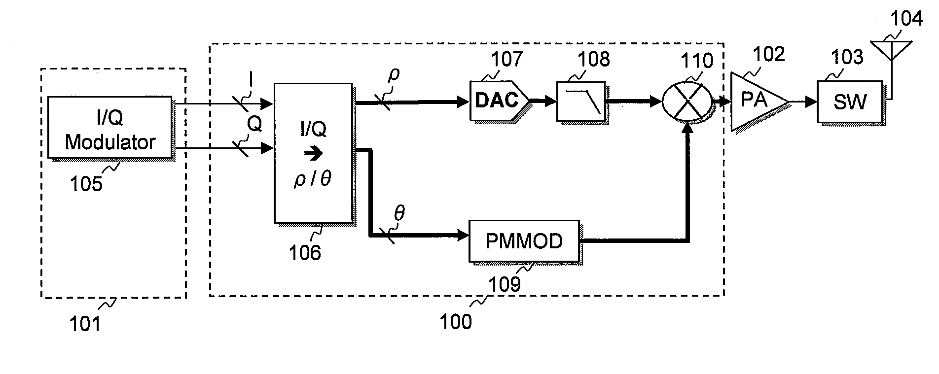
[0104]FIG. 4 is a diagram showing a structure of a polar modulation transmitter according to the first embodiment of the invention.

[0105]The polar modulation transmitter according to the first embodiment of the invention shown in FIG. 4 is equivalent to the polar modulation transmitter shown in FIG. 1 additionally provided with a signal generator 200, a delay-calibrating unit 201 and a variable delay unit 202; the polar modulation transmitter of FIG. 1 is the one which the inventors have examined prior to the invention. Therefore, the polar modulation transmitter according to the first embodiment of the invention shown in FIG. 4 has the function of matching the following two quantities with each other: a quantity of delay of an amplitude-signal path, i.e. the total quantity of delays caused by the variable delay unit 202, digital-to-analog converter (DAC) 107 and low-pass filter (LPF) 108; and a quantity of delay of a phase-signal path, i.e. the quantity of delay caused by the phas...

second embodiment

[0155]FIG. 16 is a diagram showing a structure of a polar modulation transmitter according to the second embodiment of the invention.

[0156]The difference between the polar modulation transmitter according to the second embodiment of the invention shown in FIG. 16, and the polar modulation transmitter according to the first embodiment of the invention shown in FIG. 4 will be described below.

[0157]The polar modulation transmitter according to the first embodiment of the invention shown in FIG. 4 is based on the first architecture of Polar Modulation system described in BACKGROUND OF THE INVENTION hereof, in which amplitude and phase components are synthesized by the mixer 110 located before the power amplifier (PA) 102.

[0158]In contrast, the polar modulation transmitter according to the second embodiment of the invention shown in FIG. 16 is based on the second architecture of Polar Modulation described in BACKGROUND OF THE INVENTION hereof, in which the output power of the power ampli...

third embodiment

[0161]FIG. 17 is a diagram showing a structure of a polar modulation transmitter according to the third embodiment of the invention.

[0162]The difference between the polar modulation transmitter according to the third embodiment of the invention shown in FIG. 17, and the polar modulation transmitter according to the first embodiment of the invention shown in FIG. 4 will be described below.

[0163]With the polar modulation transmitter according to the third embodiment of the invention shown in FIG. 17, the signal generator 200, which is included in RFIC 100 in the polar modulation transmitter as shown in FIG. 4, is provided in the baseband processor 101. As to the polar modulation transmitter according to the third embodiment of the invention as shown in FIG. 17, in the operation of delay calibration, a signal from the signal generator 200 in the baseband processor 101 is provided to the I / Q signal modulator 105, and I (inphase) signals and Q (quadrature) signals generated by the I / Q si...


PUM


Abstract

The transmitter synthesizes amplitude and phase components and calibrates a delay mismatch between amplitude and phase components with high accuracy at high speed. The transmitter has: a digital-to-analog converter (DAC) and a low-pass filter (LPF) in its amplitude-signal path; and a phase modulator operable to convert up a phase component into an RF component in its phase-signal path. In an operation of delay calibration, a test input signal is supplied to a delay-calibrating unit in the amplitude-signal path, and the delay-calibrating unit provides a test input signal to DAC. Then, LPF generates a test output signal. The delay-calibrating unit detects a delay of the test output signal relative to the test input signal, calibrates an amplitude signal delay in a range from the input of the delay-calibrating unit to the output of LPF, reduces the difference between amplitude and phase signal delays of the phase modulator in the phase-signal path.

Description

CLAIM OF PRIORITY[0001]The Present application claims priority from Japanese application JP 2009-209291 filed on Sep. 10, 2009, the content of which is hereby incorporated by reference into this application.FIELD OF THE INVENTION[0002]The present invention relates to a transmitter and a semiconductor integrated circuit available for it. Particularly, it relates to a technique useful for high-speed and highly-precise calibration of a delay mismatch between an amplitude component and a phase component in a transmitter of Polar Modulation type (PM: Polar Modulation).BACKGROUND OF THE INVENTION[0003]In recent years, communication devices such as mobile-phone terminals have made progress in the integration scale of baseband processors, and there has been a trend for such communication devices to have no digital-to-analog converter (DAC) nor analog-to-digital converter (ADC) inside baseband processors for achievement of higher integration according to the scaling down and reduction in pow...

Claims


Application Information

Patent Timeline
IPC IPC(8): H04B1/04
CPCH04B1/0483H03C5/00H04B2001/0491
Inventor NORIMATSU, TAKAYASUYAMAWAKI, TAIZOAKAMINE, YUKINORIMAEDA, KOJI
Owner RENESAS ELECTRONICS CORP
Why Eureka
Try Eureka