Group III nitride semiconductor light-emitting device

Active Publication Date: 2011-03-17
TOYODA GOSEI CO LTD
View PDF5 Cites 31 Cited by
  • Summary
  • Abstract
  • Description
  • Claims
  • Application Information

AI Technical Summary

Benefits of technology

[0060]According to the eleventh aspect, since the n-electrode is in contact with the auxiliary electrode in a large area, electrical conduction is readily achieved between the auxiliary electrode and the n-electrode, and thus the area of the n-electrode can be reduced. Therefore, light emission region can be enlarged, and light output can be improved.
[0061]According to the twelfth to fifteenth aspect, since a pad portion(s) of the n-electrodes is (are) provided in a symmetrical manner, current is more effectively dif

Problems solved by technology

However, sapphire poses problems in terms of electrical conductivity and thermal conductivity.
For example, a Group III nitride semiconductor light-emitting device having a device structure formed on a sapphire substrate exhibits poor linearity in a high-current region or poor durability upon long-term operation.
Therefore, when a light-emitting device is produced from a sapphire substrate, separation of the device into chips requires an intricate process (e.g., a process of thinning the sapphire substrate), which causes an increase in production cost.
Another cause of high production cost is that a sapphire substrate itself is expensive.
Thus, light extraction performance fails to be improved sufficiently.
However, in such a case, current is not diffused sufficiently in directions parallel to the main surface of the device, and uniformity of emitted light is impaired.

Method used


Image

  • Group III nitride semiconductor light-emitting device
  • Group III nitride semiconductor light-emitting device
  • Group III nitride semiconductor light-emitting device

Examples


embodiment 1

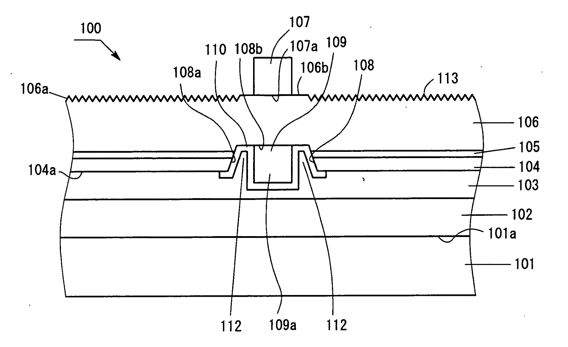
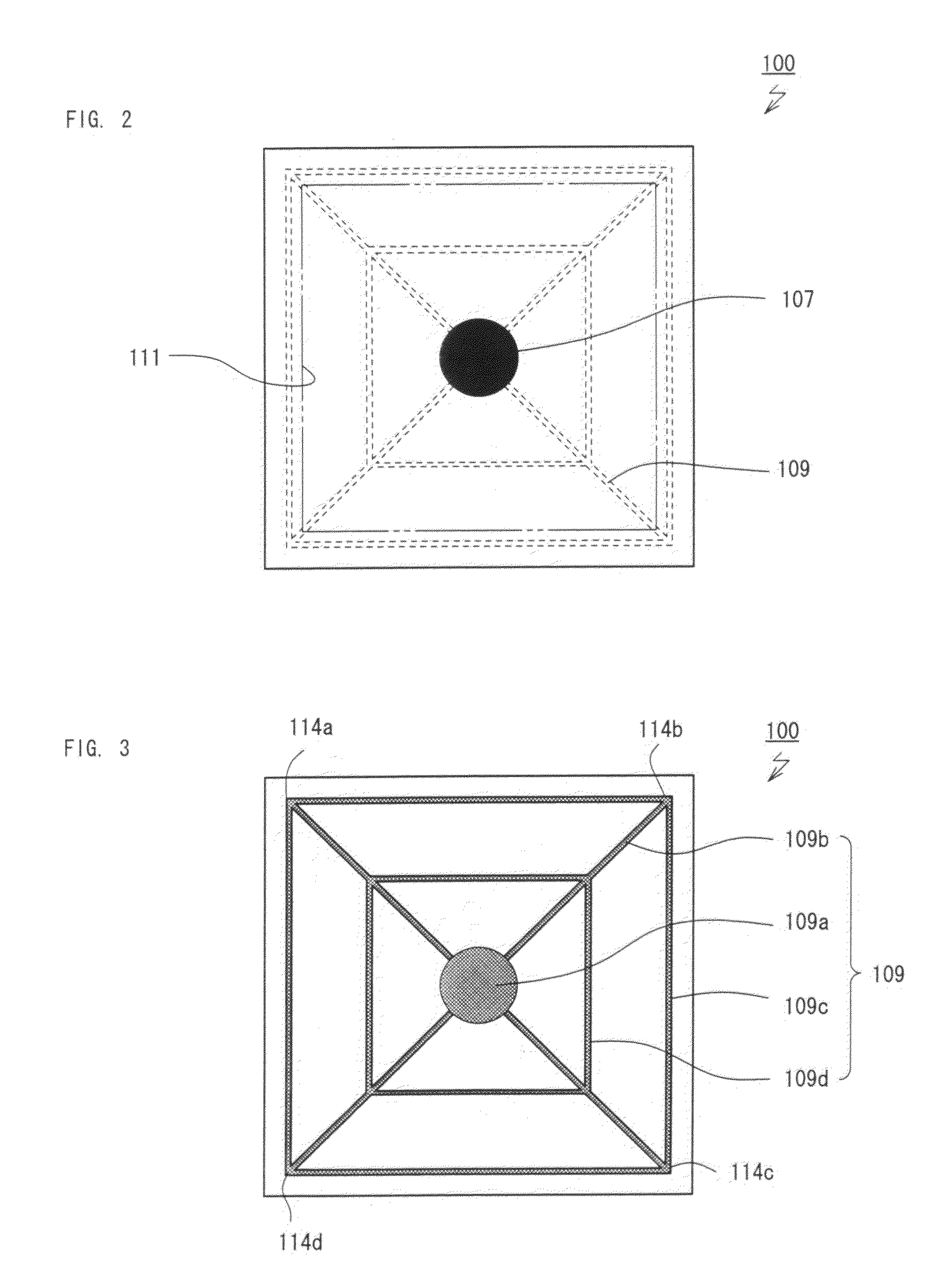
[0083]FIG. 1 is a cross-sectional view of the structure of a light-emitting device 100 according to Embodiment 1, and FIG. 2 is a top view of the light-emitting device 100. As shown in FIG. 2, the light-emitting device100 has a square form as viewed from above. As shown in FIG. 1, the light-emitting device 100 includes a support 101; a low-melting-point metal layer 102 formed on the support 101; a p-electrode 103 bonded to the support 101 via the low-melting-point metal layer 102; a p-type layer 104, an active layer 105, and an n-type layer 106, which are formed of a Group III nitride semiconductor and sequentially stacked on the p-electrode 103; and an n-electrode 107 formed on the n-type layer 106.

[0084]The support 101 may be an electrically conductive substrate formed of, for example, Si, GaAs, Cu, or Cu—W. The low-melting-point metal layer 102 may be a eutectic metal layer such as an Au—Sn layer, an Au—Si layer, an Ag—Sn—Cu layer, or an Sn—Bi layer. Alternatively, the low-meltin...

embodiment 2

[0115]In Embodiment 2, components having the same functions as those described in Embodiment 1 are denoted by the same reference numerals. FIG. 9 is a plan view of a light-emitting device 600 according to Embodiment 2, and FIG. 10 is a cross-sectional view of the device of FIG. 9, as taken along line A-A. As shown in FIG. 9, the light-emitting device 600 has a square form as viewed from above. As shown in FIG. 10, the light-emitting device 600 includes a support 101; a low-melting-point metal layer 102 formed on the support 101; a p-electrode 103 bonded to the support 101 via the low-melting-point metal layer 102; a p-type layer 104, an active layer 105, and an n-type layer 106, which are formed of a Group III nitride semiconductor and sequentially stacked on the p-electrode 103; an n-pad electrode 607; and an auxiliary electrode 609.

[0116]The support 101 may be an electrically conductive substrate formed of, for example, Si, GaAs, Cu, or Cu—W. A bottom electrode 117 is formed on th...

embodiment 3

[0139]In Embodiment 3, components having the same functions as those described in Embodiment 1 or 2 are denoted by the same reference numerals. FIG. 15 is a plan view of a light-emitting device 700 according to Embodiment 3, and FIG. 16 is a cross-sectional view of the device of FIG. 15, as taken along line A-A. As shown in FIG. 16, the light-emitting device 700 includes a ceramic substrate 701; a low-melting-point metal layer 102 formed on the ceramic substrate 701; a p-electrode 103 bonded to the ceramic substrate 701 via the low-melting-point metal layer 102; a p-type layer 104, an active layer 105, and an n-type layer 106, which are formed of a Group III nitride semiconductor and sequentially stacked on the p-electrode 103; an n-pad electrode 707; an auxiliary electrode 709; and a p-pad electrode 714. As shown in FIG. 15, the light-emitting device 700 has a square form as viewed from above, and the n-pad electrode 707 and the p-pad electrode 714 are formed on the same surface.

[0...


PUM


Abstract

A Group III nitride semiconductor light-emitting device includes an electrically conductive support; a p-electrode provided on the support; a p-type layer, an active layer, and an n-type layer, which are formed of a Group III nitride semiconductor and are sequentially provided on the p-electrode; an n-electrode which is connected to the n-type layer; a first trench extending from the surface of the p-type layer on the p-electrode's side to reach the n-type layer; an auxiliary electrode which is in contact with the surface of the n-type layer serving as the bottom of the first trench, but is not in contact with the side walls of the first trench; and an insulating film which exhibits light permeability and covers the auxiliary electrode and the bottom and side walls of the first trench.

Description

BACKGROUND OF THE INVENTION[0001]1. Field of the Invention[0002]The present invention relates to a Group III nitride semiconductor light-emitting device including an epitaxially grown layer which has been removed from a growth substrate through the lift-off process and is bonded to a support. The present invention also relates to a light-emitting device including a support formed of a ceramic substrate.[0003]2. Background Art[0004]In general, a sapphire substrate has been used as a growth substrate for a Group III nitride semiconductor. However, sapphire poses problems in terms of electrical conductivity and thermal conductivity. For example, a Group III nitride semiconductor light-emitting device having a device structure formed on a sapphire substrate exhibits poor linearity in a high-current region or poor durability upon long-term operation. Sapphire has no cleavage property and exhibits high physical and chemical strength. Therefore, when a light-emitting device is produced fro...

Claims


Application Information

Patent Timeline
IPC IPC(8): H01L33/40
CPCH01L33/38H01L33/44H01L2924/0002H01L2924/00
Inventor UEMURA, TOSHIYAITO, JUN
Owner TOYODA GOSEI CO LTD
Why Eureka
Try Eureka