Growth Structures and Method for Forming Laser Diodes on or Off Cut Gallium and Nitrogen Containing Substrates

a growth structure and laser diode technology, applied in the field of optical devices, can solve the problems of ineffective illumination, routine failure of the bulb, and drawbacks of the conventional edison light bulb, and achieve the effect of improving the cleavage structure of the laser device and cost-effectiveness

Active Publication Date: 2011-03-17
KYOCERA SLD LASER INC
View PDF100 Cites 250 Cited by
  • Summary
  • Abstract
  • Description
  • Claims
  • Application Information

AI Technical Summary

Benefits of technology

[0017]The present invention enables a cost-effective optical device for laser applications. The optical device can be manufactured in a relatively simple and cost effective manner using commercially available equipment. The laser device uses a semipolar gallium nitride material to achieve a green laser device. In one or more embodiments, the laser device is capable of emitting long wavelengths such...

Problems solved by technology

Unfortunately, drawbacks exist with the conventional Edison light bulb.
Reliability is also an issue since the bulb routinely fails due to thermal expansion and contraction of the filament element.
In addition, light bulbs emit light over a broad spectrum, much of which does not result in useful illumination due to the spectral sensitivity of the human eye.
Another disadvantage is that light bulbs emit light in all directions.
Thus they are not ideal for applications requiring strong directionality or focus, such as projection displays, optical data storage, or specialized directed lighting.
The wall plug efficiency, however, was less than 1 percent, and the size, weight, and cost of the lasers were undesirable as well.
As laser technology evolved, more efficient lamp pumped solid state laser designs were developed for the red and infrared wavelengths, but these technologies remained a challenge for blue and green and blue...

Method used


Image

  • Growth Structures and Method for Forming Laser Diodes on  or Off Cut Gallium and Nitrogen Containing Substrates
  • Growth Structures and Method for Forming Laser Diodes on  or Off Cut Gallium and Nitrogen Containing Substrates
  • Growth Structures and Method for Forming Laser Diodes on  or Off Cut Gallium and Nitrogen Containing Substrates

Examples


Embodiment Construction

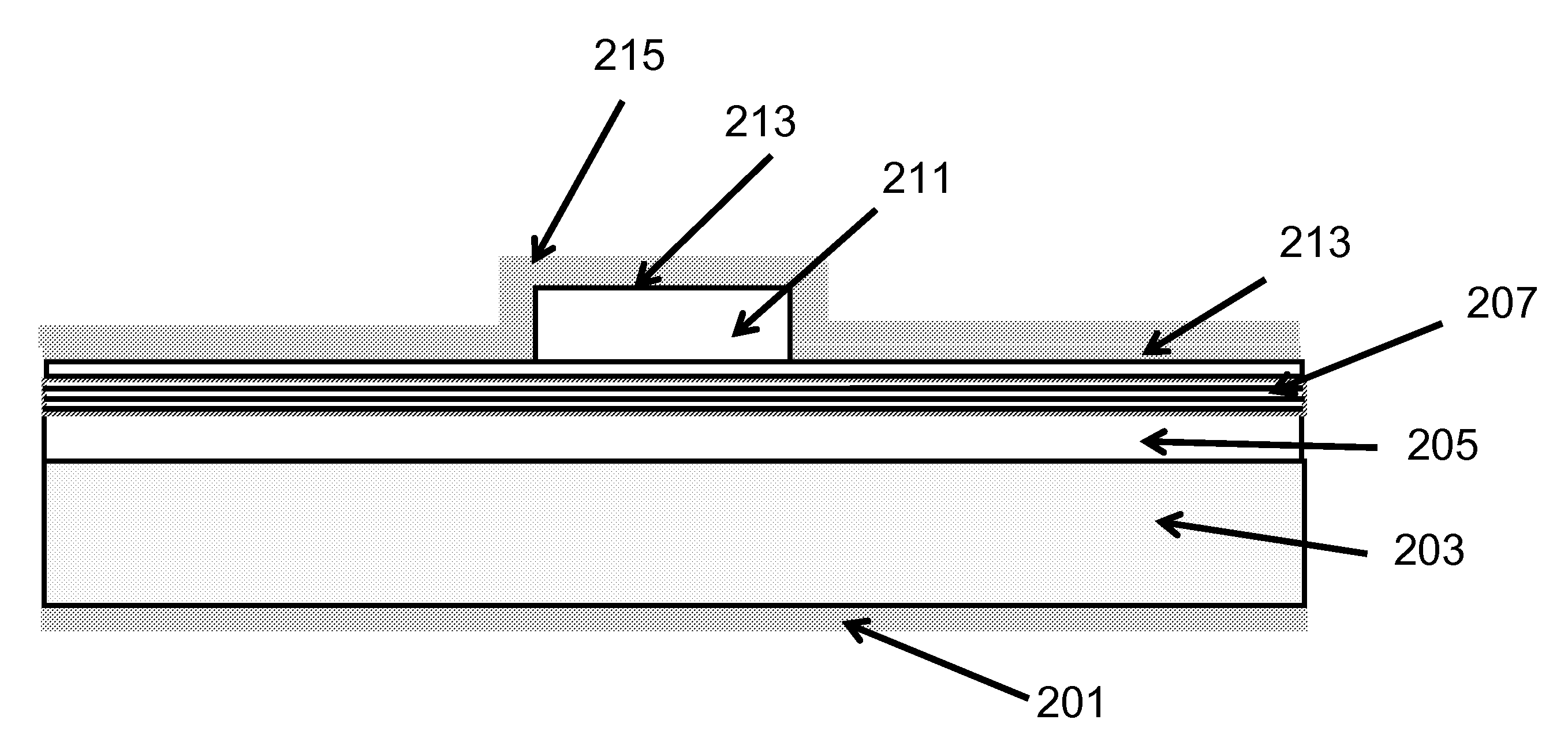
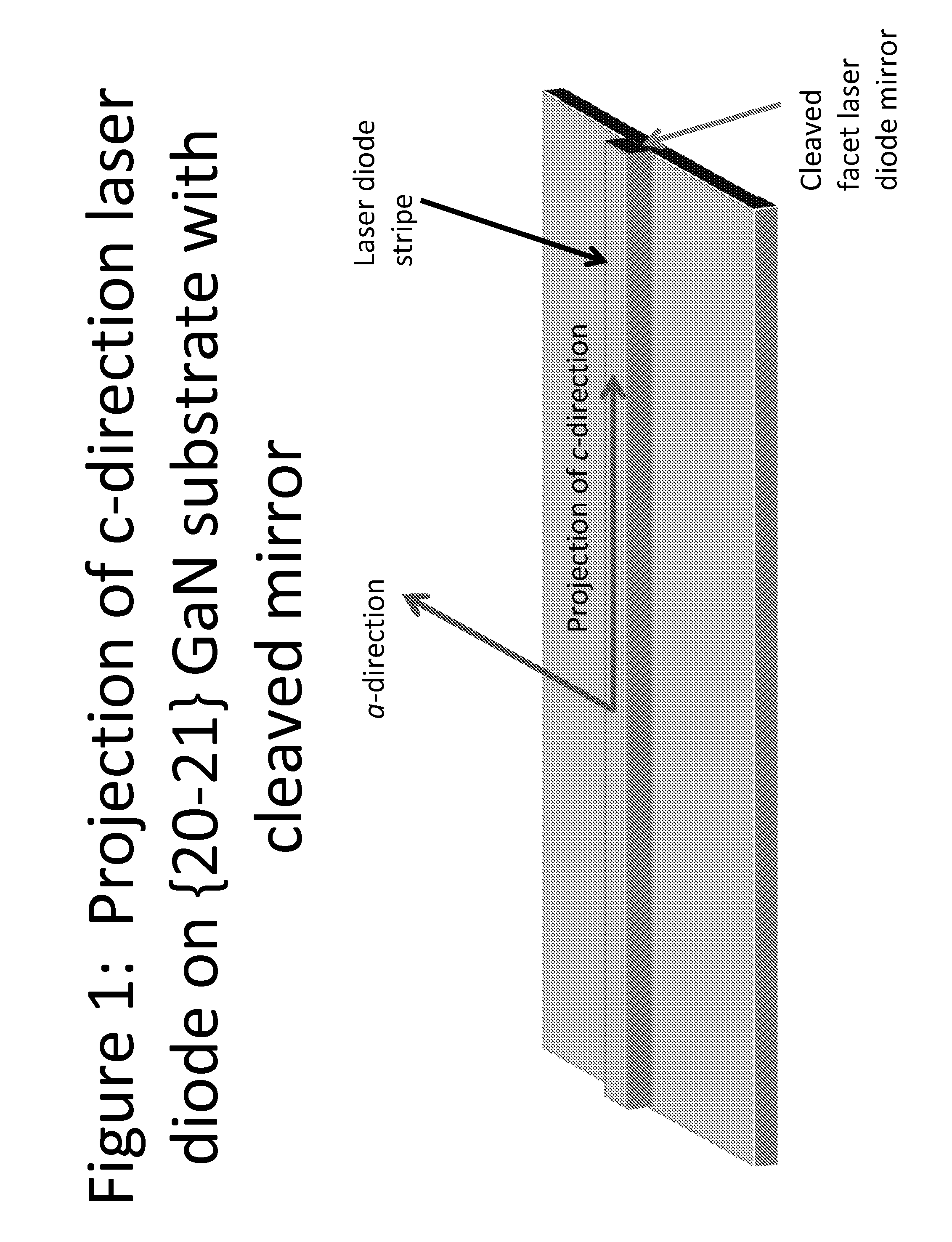
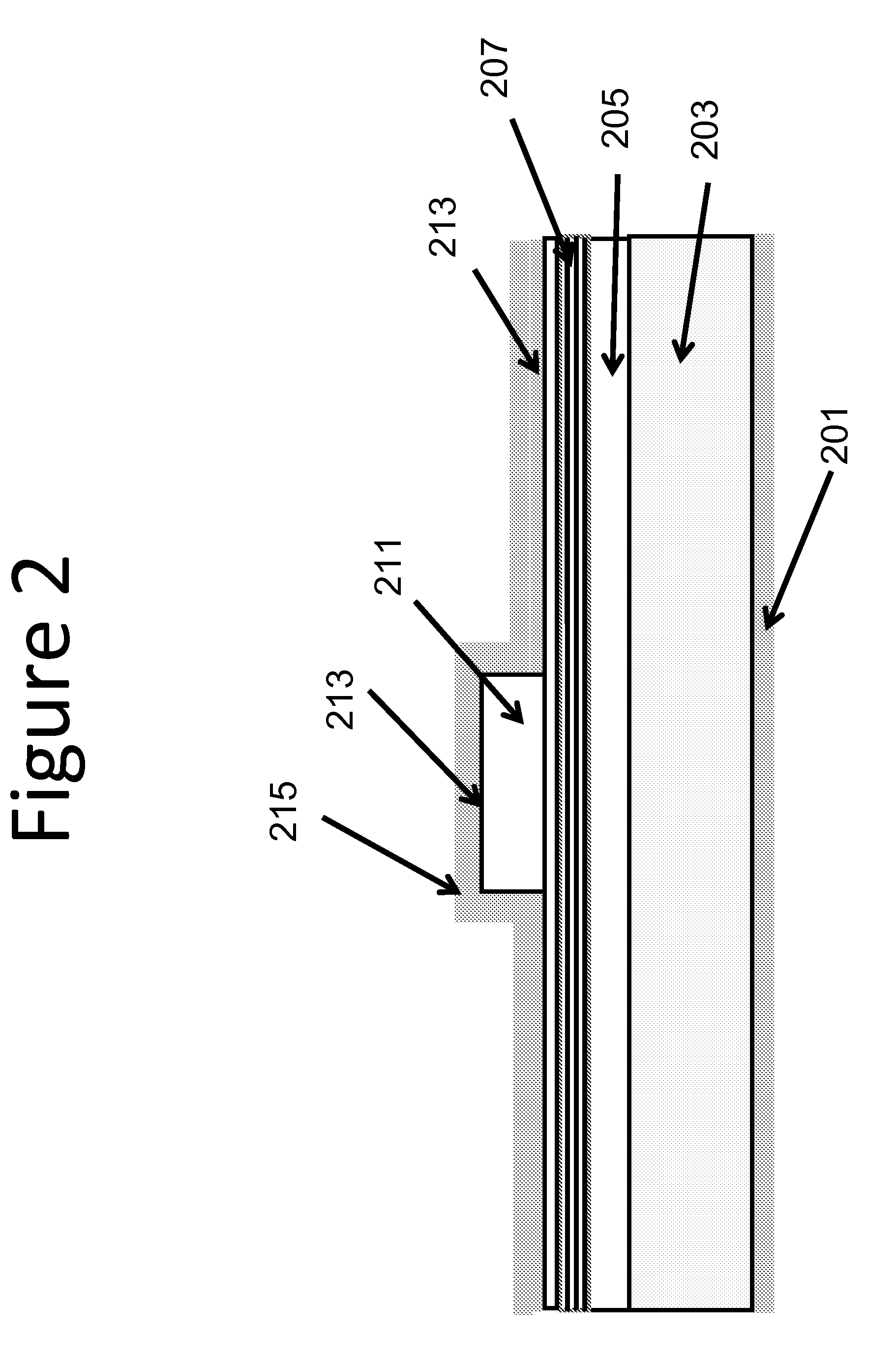
[0032]We have explored epitaxial growth and cleave properties on semipolar crystal planes oriented between the nonpolar m-plane and the polar c-plane. In particular, we have grown on the {30-31} and {20-21} families of crystal planes. We have achieved epitaxy structures and cleaves that create a path to efficient laser diodes operating at wavelengths from about 400 nm to green, e.g., 500 nm to 540 nm. These results include bright blue epitaxy in the 450 nm range, bright green epitaxy in the 520 nm range, and smooth naturally occurring cleave planes orthogonal to the projection of the c-direction. It is desirable to align the laser cavities parallel to the projection of the c-direction for maximum gain on this family of crystal planes.

[0033]Although it was believed that a higher gain would be offered in the projection of the c-direction than would be available in the a-direction, it is also desirable to form a high quality cleavage plane orthogonal to a stripe oriented in the project...


PUM


Abstract

An optical device having a structured active region configured for one or more selected wavelengths of light emissions and formed on an off-cut m-plane gallium and nitrogen containing substrate.

Description

CROSS-REFERENCE TO RELATED APPLICATIONS[0001]This application claims priority to U.S. Application Nos. 61 / 243,502, filed Sep. 17, 2009, and 61 / 249,568, filed Oct. 7, 2009, each of which is incorporated by reference in its entirety.BACKGROUND OF THE INVENTION[0002]This invention is directed to optical devices. In particular, the invention provides a method of manufacture and a device for emitting electromagnetic radiation using nonpolar or semipolar gallium containing substrates, such as GaN, AlN, InN, InGaN, AlGaN, and AlInGaN, and others. More particularly, the invention provides a device using a gallium and nitrogen containing substrate configured on the {20-21} family of planes or an off-cut of the {20-21} family of planes towards the c-plane and / or towards the a-plane. The invention can be applied to optical devices, lasers, light emitting diodes, solar cells, photoelectrochemical water splitting and hydrogen generation, photodetectors, integrated circuits, and transistors, as w...

Claims


Application Information

Patent Timeline
IPC IPC(8): H01S5/323H01S5/22H01S5/34H01L21/302
CPCB82Y20/00H01S5/0014H01S5/0202H01S5/028H01S5/4025H01S5/3202H01S5/3213H01S5/34333H01S5/2009H01S5/2201H01S5/32025H01S5/320275B28D5/0011H01L21/02389H01L21/02433H01L21/0254H01L21/467H01S5/227H01S5/3407
Inventor RARING, JAMES W.PFISTER, NICKSCHMIDT, MATHEWPOBLENZ, CHRISTIANE
Owner KYOCERA SLD LASER INC
Why Eureka
Try Eureka