Laser diodes with scribe structures

a laser diode and scribe technology, applied in the field of optical devices, can solve the problems of reducing the efficiency of the wall plug, reducing affecting so as to improve the cleavage of the laser device structure, and improve the efficiency of the laser device. the effect of cost-effectiveness

Active Publication Date: 2014-10-23
KYOCERA SLD LASER INC
View PDF2 Cites 4 Cited by
  • Summary
  • Abstract
  • Description
  • Claims
  • Application Information

AI Technical Summary

Benefits of technology

[0008]This invention is directed to optical devices and related methods. In particular, the invention provides a method and device for emitting electromagnetic radiation using semi-polar or non-polar gallium containing substrates. More particularly, the invention provides a method and device using a gallium and nitrogen containing substrate where the backside of the substrate includes multiple trench structures that reduce stray light leaking The invention is readily applicable to optical devices such as lasers, light emitting diodes, solar cells, and photodetectors.
[0012]The present invention enables a cost-effective optical device for laser applications. In a specific embodiment, the present optical device can be manufactured in a relatively simple and cost effective manner. Depending upon the embodiment, the present apparatus and method can be manufactured using conventional materials and / or methods. The laser device uses a nonpolar or semipolar gallium nitride material capable of achieving a violet or blue or green emission, among others. In some embodiments, the laser device is capable of emitting long wavelengths such as those ranging from about 430 nm to 470 nm for the blue wavelength region or 500 nm to about 540 nm for the green wavelength region, but can be others such as the violet region. In a specific embodiment, the present method and structure uses a top-side skip and scribe technique for improved cleaves in the laser device structure. In one or more embodiments, the present invention provides a method using a top side skip-scribe technique for good facets oriented substantially orthogonal to the laser cavities, where the laser cavity is oriented in the c-direction or in the projection of the c-direction. It is to be understood that the trench structures according to the present invention can be used in other types of laser devices, such as laser device having polar orientation, such as a laser fabricated on c-plane GaN. The trench structures are relatively easy and inexpensive to form. In a specific embodiment, the present method and structure improves device performance by reducing leakage light, interference patterns, and other undesirable characteristics of laser devices.

Problems solved by technology

The Ar-ion laser had the benefit of producing highly directional and focusable light with a narrow spectral output, but the wall plug efficiency was <0.1%, and the size, weight, and cost of the lasers were undesirable as well.
As laser technology evolved, more efficient lamp pumped solid state laser designs were developed for the red and infrared wavelengths, but these technologies remained a challenge for blue and green and blue lasers.
The resulting green and blue lasers were called “lamped pumped solid state lasers with second harmonic generation” (LPSS with SHG) had wall plug efficiency of ˜1%, and were more efficient than Ar-ion gas lasers, but were still too inefficient, large, expensive, fragile for broad deployment outside of specialty scientific and medical applications.
Additionally, the gain crystal used in the solid state lasers typically had energy storage properties which made the lasers difficult to modulate at high speeds which limited its broader deployment.
However, the change to diode pumping increased the system cost and required precise temperature controls, leaving the laser with substantial size, power consumption while not addressing the energy storage properties which made the lasers difficult to modulate at high speeds.
These lasers designs are meant to improve the efficiency, cost and size compared to DPSS-SHG lasers, but the specialty diodes and crystals required make this challenging today.
Additionally, while the diode-SHG lasers have the benefit of being directly modulate-able, they suffer from severe sensitivity to temperature, which limits their application.
One factor that often affects laser performance is straying light.
For example, straying light is not usable for intended purposes and often interferes with the laser beam output.

Method used


Image

  • Laser diodes with scribe structures
  • Laser diodes with scribe structures
  • Laser diodes with scribe structures

Examples


Embodiment Construction

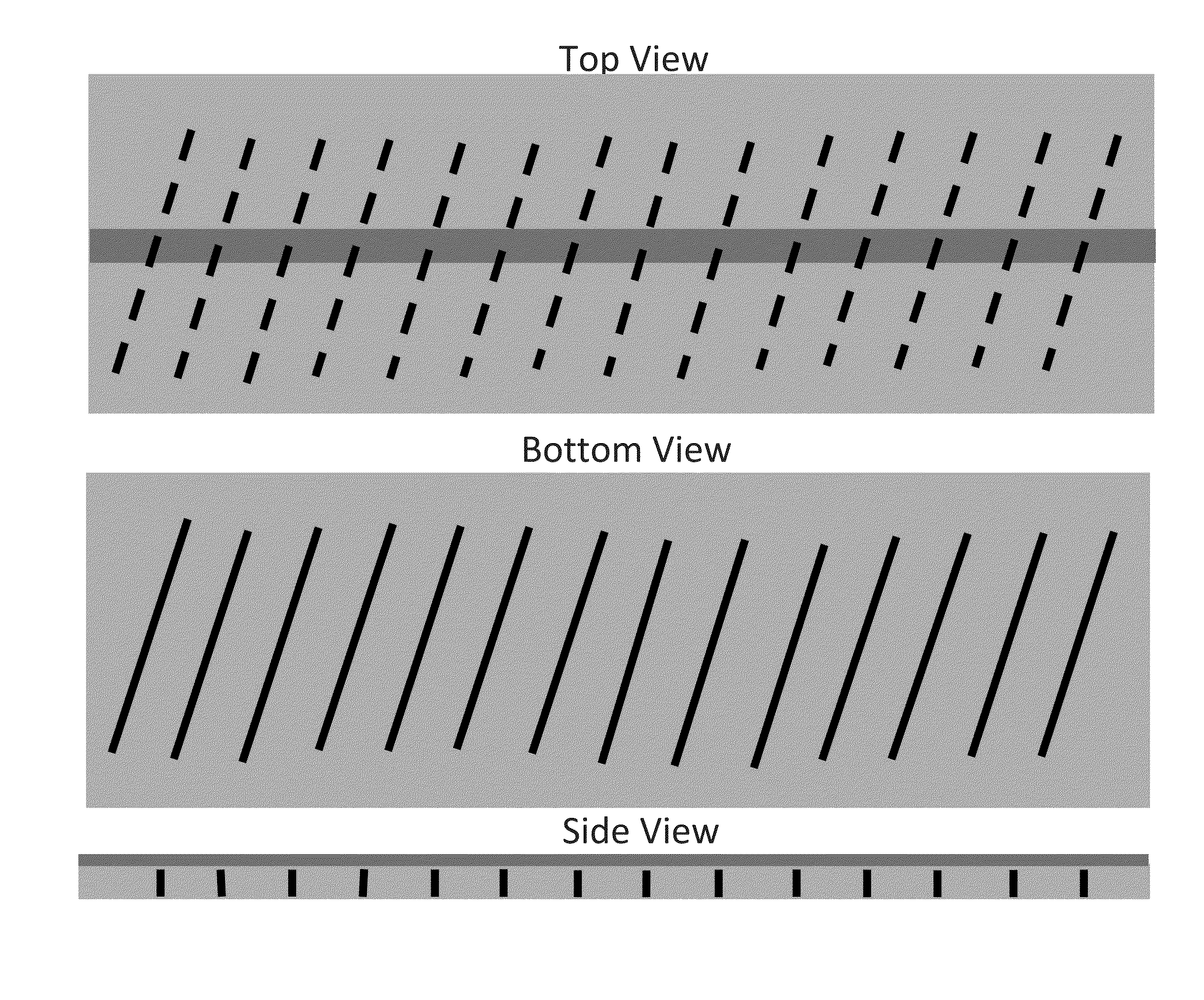
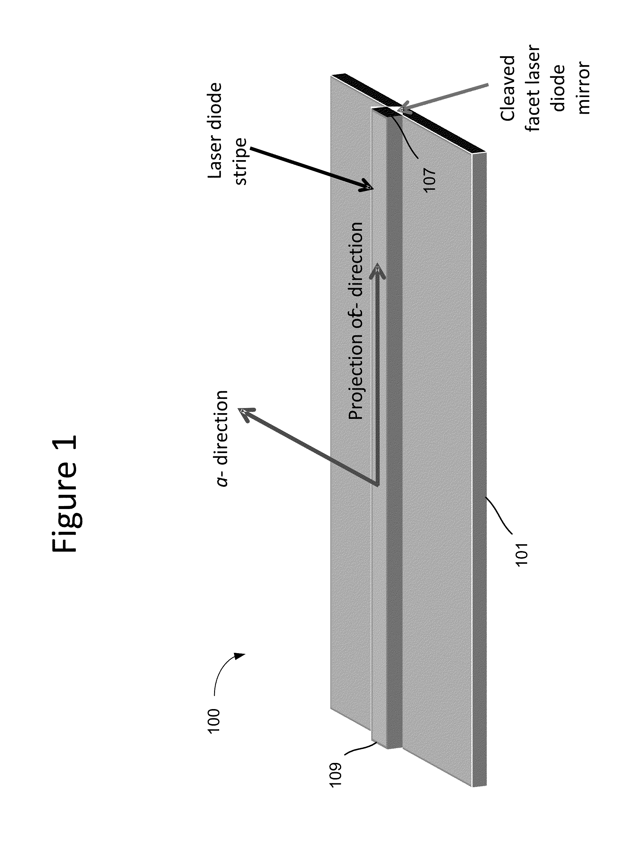
[0026]FIG. 1 is a perspective view of a laser device 100 fabricated on a bulk substrate according to an embodiment of the present invention. In an exemplary embodiment, the optical device includes a gallium nitride substrate 101 having a non-polar crystalline surface region characterized by an orientation of about −2 degrees to about 2 degrees towards (000-1) and less than about 0.5 degrees towards (11-20). In a specific embodiment, the gallium nitride substrate is a bulk GaN substrate having a nonpolar crystalline surface region. In certain embodiment, the substrate is characterized by a semi-polar orientation. In a specific embodiment, the bulk GaN substrate has a surface dislocation density below 105 cm−2 or 10E5 to 10E7 cm-2. The nitride crystal or wafer may comprise AlxInyGa1-x-yN, where 0≦x, y, x+y≦1. In one specific embodiment, the nitride crystal comprises GaN. In one or more embodiments, the GaN substrate has threading dislocations, at a concentration between about 105 cm−2...


PUM


Abstract

A method and device for emitting electromagnetic radiation using semipolar or nonpolar gallium containing substrates is described where the backside of the substrate includes multiple scribes that reduce stray light leaking.

Description

CROSS-REFERENCE TO RELATED APPLICATIONS[0001]The present application is a divisional of U.S. application Ser. No. 13 / 363,935, filed Feb. 1, 2012, which claims priority to U.S. Application Ser. No. 61 / 533,030, filed Sep. 9, 2011; which is related to U.S. Provisional Application No. 61 / 243,502, filed Sep. 17, 2009; U.S. Provisional Application No. 61 / 249,568, filed Oct. 7, 2009; and to U.S. Provisional Application No. 61 / 367,036, filed Jul. 23, 2010; each of which is incorporated by reference herein for all purposes.BACKGROUND OF THE INVENTION[0002]This invention is directed to optical devices and related methods. In particular, the invention provides a method and device for emitting electromagnetic radiation using semi-polar or non-polar gallium containing substrates. More particularly, the invention provides a method and device using a gallium and nitrogen containing substrate where the backside of the substrate includes multiple trench structures that reduce stray light leaking The...

Claims


Application Information

Patent Timeline
Patent Type & Authority Applications(United States)
IPC IPC(8): H01L33/00
CPCH01L33/005H01S5/0202H01S5/1039H01S5/34333H01S5/3063H01S2301/14H01S5/2201H01S5/320275H01S5/0206H01S5/0207H01L21/02016H01L21/268H01L21/302H01L21/428H01L33/0062H01L33/0095H01L33/20H01S5/22
Inventor RARING, JAMES W.PFISTER, NICKCHANG, YU-CHIASCHMIDT, MATHEW C.FELKER, DREW
Owner KYOCERA SLD LASER INC
Why Eureka
Try Eureka