Method for cleaning with fluorine compound

a fluorine compound and cleaning method technology, applied in the field of cleaning methods, can solve the problems of inability to obtain high-level cleaning effects and achieve the effect of high-level cleaning

Inactive Publication Date: 2011-03-24
ASAHI GLASS CO LTD
View PDF6 Cites 9 Cited by
  • Summary
  • Abstract
  • Description
  • Claims
  • Application Information

AI Technical Summary

Benefits of technology

[0024]According to the cleaning method of the present invention, an object to be cleaned having a plasma polymer formed in a plasma etching step employing a fluorinated gas can be favorably removed, and the cleaning method of the present invention is suitably employed in a process for producing various substrates such as large-scale integrated circuits (LSI).

Problems solved by technology

However, by a conventional cleaning method using a fluorinated solvent, a high level cleaning effect to such an extent that the plasma-polymerized film can favorably be removed, cannot be obtained.

Method used


Image

  • Method for cleaning with fluorine compound
  • Method for cleaning with fluorine compound
  • Method for cleaning with fluorine compound

Examples


first embodiment

A. Examples for the Present Invention

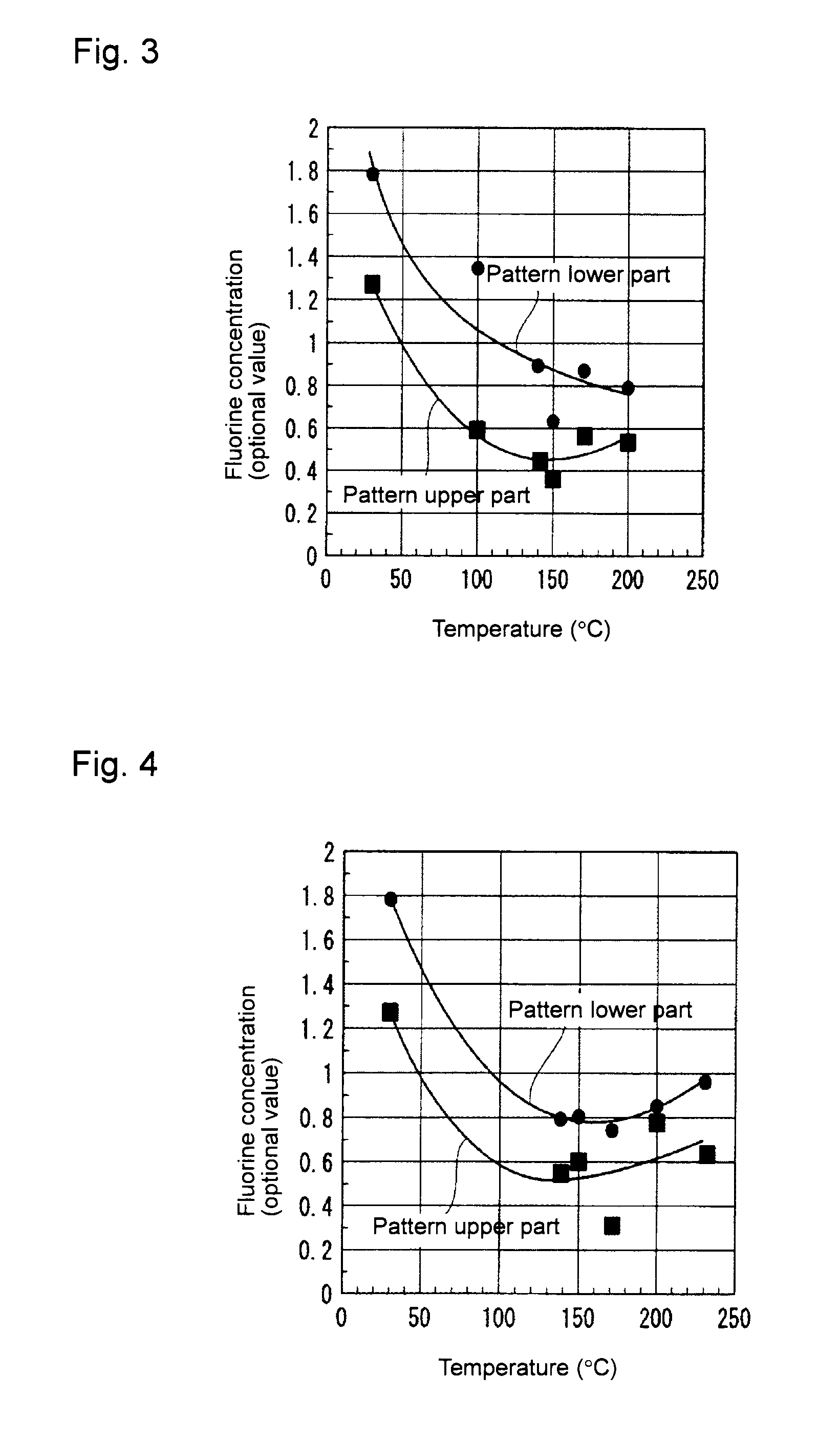
[0162]In Table 2 are shown cleaning effects when a plasma-polymerized film was cleaned by using fluorinated solvents comprising various fluorine compounds. The fluorinated solvent (cleaning liquid) comprises 100 mass % of a fluorine compound shown in Table 2. As an object to be cleaned, a plasma-polymerized film (solid film not patterned) having a thickness of from 800 to 900 nm deposited on a silicon substrate using C4F8 gas plasma was used.

[0163]Details under “Cleaning conditions” shown in Table 2 are shown below.

[Cleaning Conditions]

[0164](1) 30° C.: A substrate was immersed in a fluorinated solvent having its temperature adjusted to 30° C. under atmospheric pressure for 60 minutes, and then dried by heating in an oven at 120° C. for 1 hour.[0165](2) Boiling: A substrate was immersed in a fluorinated solvent in a boiling state by being heated to the normal boiling point or higher under atmospheric pressure for 1 hour, and then taken out.[0166]...

example 1

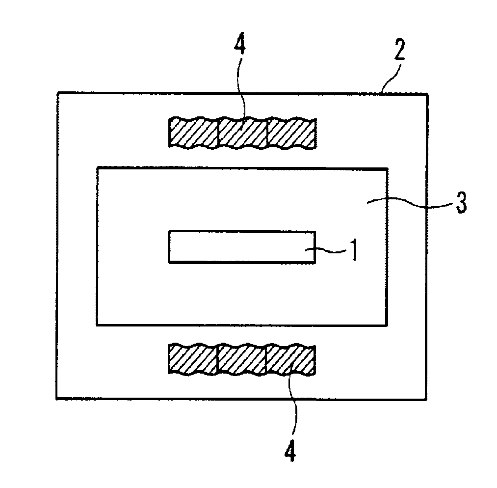
[0189]On a silicon substrate, a resist pattern having a width of from 50 to 300 mm was formed by known photolithography. This silicon substrate was etched by alternate treatment with SF6 gas plasma and C4F8 gas plasma to form a pattern comprising silicon.

[0190]Then, the substrate was placed in a container capable of being closed, and a fluorinated solvent comprising C6F13CH2CH3 (Test Example 7) was introduced into the container so that the substrate was immersed in the fluorinated solvent.

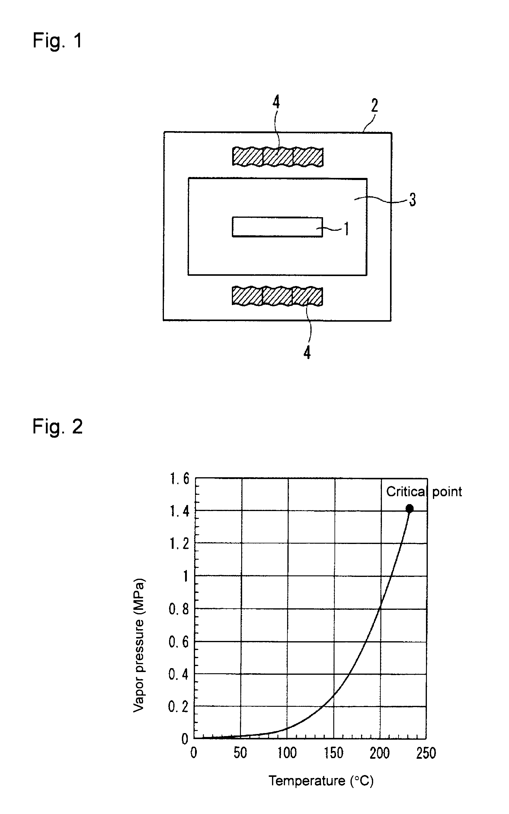
[0191]The container was closed, and the temperature in the container and the temperature of the fluorinated solvent were raised to 170° C. and in addition, the container was closed and the pressure in the container was adjusted to 0.5 MPa by a back pressure valve, whereby the fluorinated solvent was converted to a liquid at high temperature of at least the normal boiling point (hereinafter referred to as a high temperature liquid). 30 Minutes later, while the temperature in the closed container was...

example 2

[0193]A substrate was immersed in a fluorinated solvent for 30 minutes in the same manner as in Example 1, and then the heater of the closed container was turned off and in addition, the fluorinated solvent was discharged outside the closed container, and the container was taken out from the substrate. The taken out substrate was heated to 100° C. under vacuum of 0.1 Pa, and the fluorinated solvent remaining on the substrate surface was vaporized to dry the substrate.

[0194]On the substrate after cleaning, the plasma-polymerized film attached to the pattern side wall was dissolved and removed.


PUM


Abstract

To provide a cleaning method capable of favorably removing an object to be cleaned having a plasma polymer formed in a plasma etching step employing a fluorinated gas.
A cleaning method comprising an immersion step of immersing an object 1 to be cleaned in a cleaning liquid (fluorinated solvent) 3 containing at least a fluorine compound, wherein in the immersion step, the temperature t of the cleaning liquid 3 is at least the lower one of the normal boiling point of the fluorine compound contained in the cleaning liquid 3 at 1 atm and 100° C., and the atmospheric pressure is such a pressure that the fluorine compound is in a liquid state at the temperature t. Further, a cleaning method comprising an immersion step of immersing an object to be cleaned having a plasma polymer formed in a plasma etching step employing a fluorinated gas, in a cleaning liquid containing a fluorinated compound, wherein the fluorinated compound has a linear or branched perfluoroalkyl group having a number of carbon atoms of at least 5.

Description

TECHNICAL FIELD[0001]The present invention relates to a cleaning method suitably employed in a process for producing various substrates such as microelectromechanical systems (MEMS) and large-scale integrated circuits (LSI).BACKGROUND ART[0002]For production of LSI and MEMS, a fine pattern is required. Such a fine pattern is an etching pattern formed by etching using, as a mask, a resist pattern formed by means of exposure, development and rinsing, followed by cleaning. For the etching, plasma etching using a fluorinated gas is mainly employed. In order to improve the pattern dimensional accuracy in the plasma etching, it is required to carry out etching while a plasma-polymerized film is deposited on side walls of the pattern, whereby the side etching which occurs at the time of etching can be prevented. The side etching is diffusion of a reaction species (such as a fluorine radical) formed by the gas plasma in the lateral direction to increase the pattern dimensions.[0003]For exam...

Claims


Application Information

Patent Timeline
Patent Type & Authority Applications(United States)
IPC IPC(8): B08B3/00
CPCC11D7/5018C11D11/0047H05K2203/095H01L21/02063H05K3/26H01L21/02057
Inventor OKAMOTO, HIDEKAZUNAMATSU, HIDEO
Owner ASAHI GLASS CO LTD
Why Eureka
Try Eureka