Process for bonding and transferring a layer
- Summary
- Abstract
- Description
- Claims
- Application Information
AI Technical Summary
Benefits of technology
Problems solved by technology
Method used
Image

Examples
example 1
Fabrication of an SOI Comprising Electronic Components
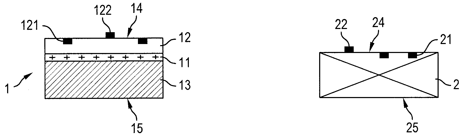
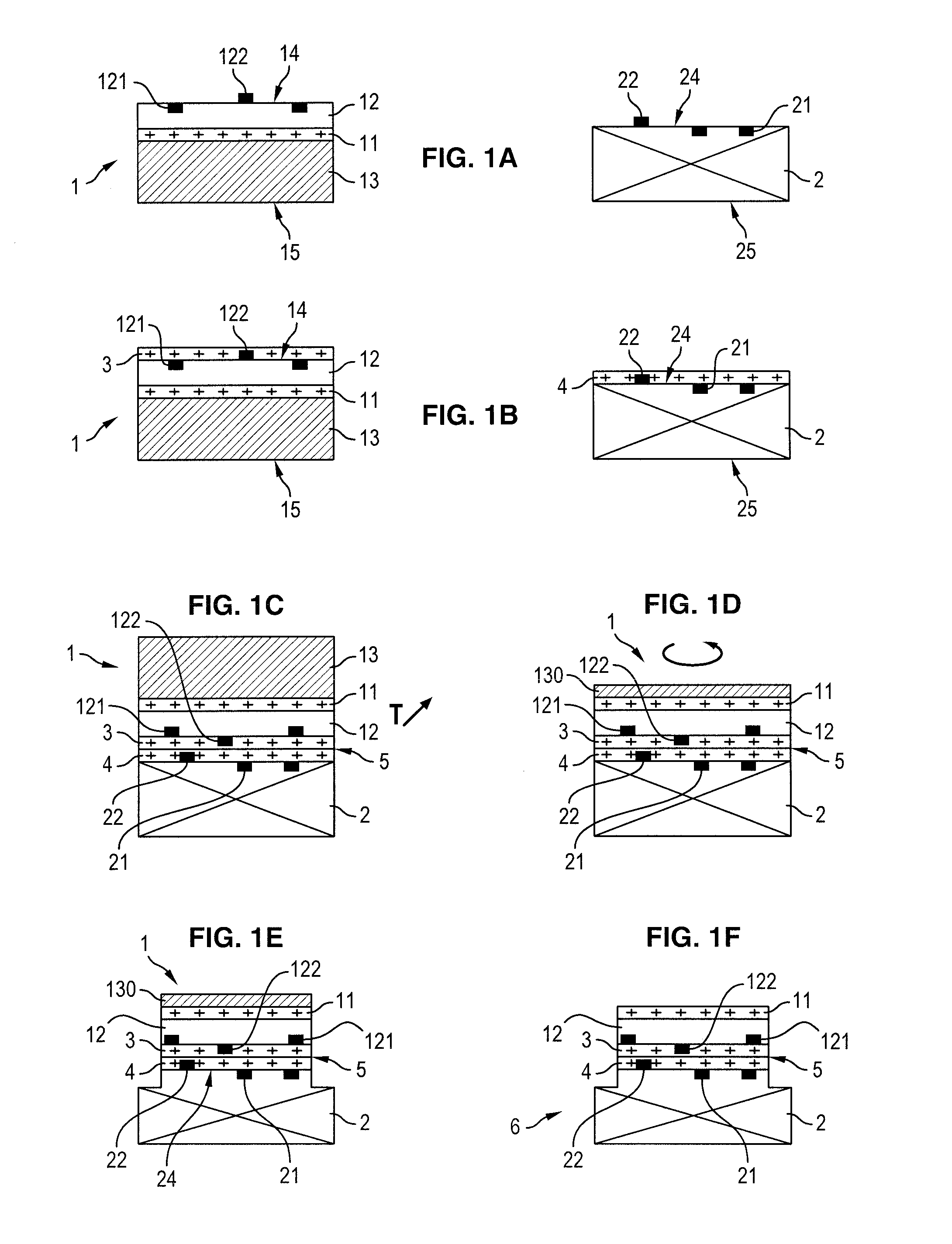
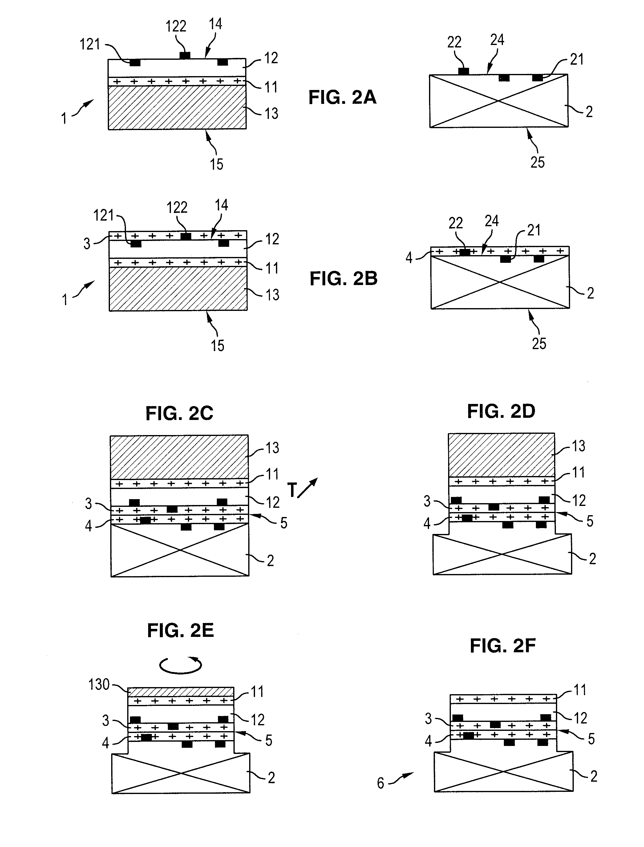
[0098]A silicon receiver substrate has been oxidized and a layer of oxide has been deposited at low temperature (between 200° C. and 500° C.) onto a donor substrate of the SOI type comprising electronic components.
[0099]The donor substrate has been planarized until a surface condition is obtained that is compatible with direct bonding by molecular adhesion, in other words until a roughness of less than 3 Å RMS (3 angströms) has been obtained for a scan width of 2 μm by 2 μm.
[0100]After cleaning and surface activation, the two substrates have been assembled. The bonded structure has then been subjected to a heat treatment at 350° C. for 1 hour, in order to consolidate the bonding interface.
[0101]The back face of the donor substrate has then been thinned by grinding down to around 35 μm. The trimming step has subsequently been applied to around 3 mm from the edge of the substrate.
[0102]This structure has then been immersed in a sol...
example 2
Fabrication of an SOI Using a Bulk Donor Substrate
[0103]After having carried out the oxidation of a silicon receiver substrate, it is bonded with a donor substrate also made of silicon.
[0104]The assembly has been subjected to an annealing step for stabilization of the bonding, using a heat treatment at 1100° C. for 2 hours under an oxygen atmosphere.
[0105]The thinning of the donor substrate has subsequently been carried out then the trimming of the stack over a 0.5 to 3 mm width, and 2 to 10 micrometers depth into the support.
[0106]Following this, an etch has been performed by means of TMAH (concentration 25% by weight in water, temperature 60° C.), in such a manner as to remove the area work-damaged by the thinning step, in other words the exposed surface of the donor substrate remnant, and to process the faces exposed by the receiver substrate trimming step. This etch step results in the removal of around 0.5 to 2 micrometers of the thickness.
[0107]Lastly, a final polishing of the...
PUM
| Property | Measurement | Unit |
|---|---|---|
| Temperature | aaaaa | aaaaa |
| Temperature | aaaaa | aaaaa |
| Thickness | aaaaa | aaaaa |
Abstract
Description
Claims
Application Information
 - Generate Ideas
- Intellectual Property
- Life Sciences
- Materials
- Tech Scout
- Unparalleled Data Quality
- Higher Quality Content
- 60% Fewer Hallucinations
Browse by: Latest US Patents, China's latest patents, Technical Efficacy Thesaurus, Application Domain, Technology Topic, Popular Technical Reports.
© 2025 PatSnap. All rights reserved.Legal|Privacy policy|Modern Slavery Act Transparency Statement|Sitemap|About US| Contact US: help@patsnap.com