Imaging system

a technology of imaging system and image, applied in the field of imaging system, can solve problems such as limited physical dimensions, and achieve the effects of reducing spot size, high resolution, and sufficient wafer throughpu

a technology of imaging system and image, applied in the field of imaging system, can solve problems such as limited physical dimensions, and achieve the effects of reducing spot size, high resolution, and sufficient wafer throughpu

US20110079730A1Active Publication Date: 2011-04-07ASML NETHERLANDS BV

Image

  • Imaging system
  • Imaging system
  • Imaging system

Examples


Embodiment Construction

[0023]The following is a description of various embodiments of the invention, given by way of example only and with reference to the drawings.

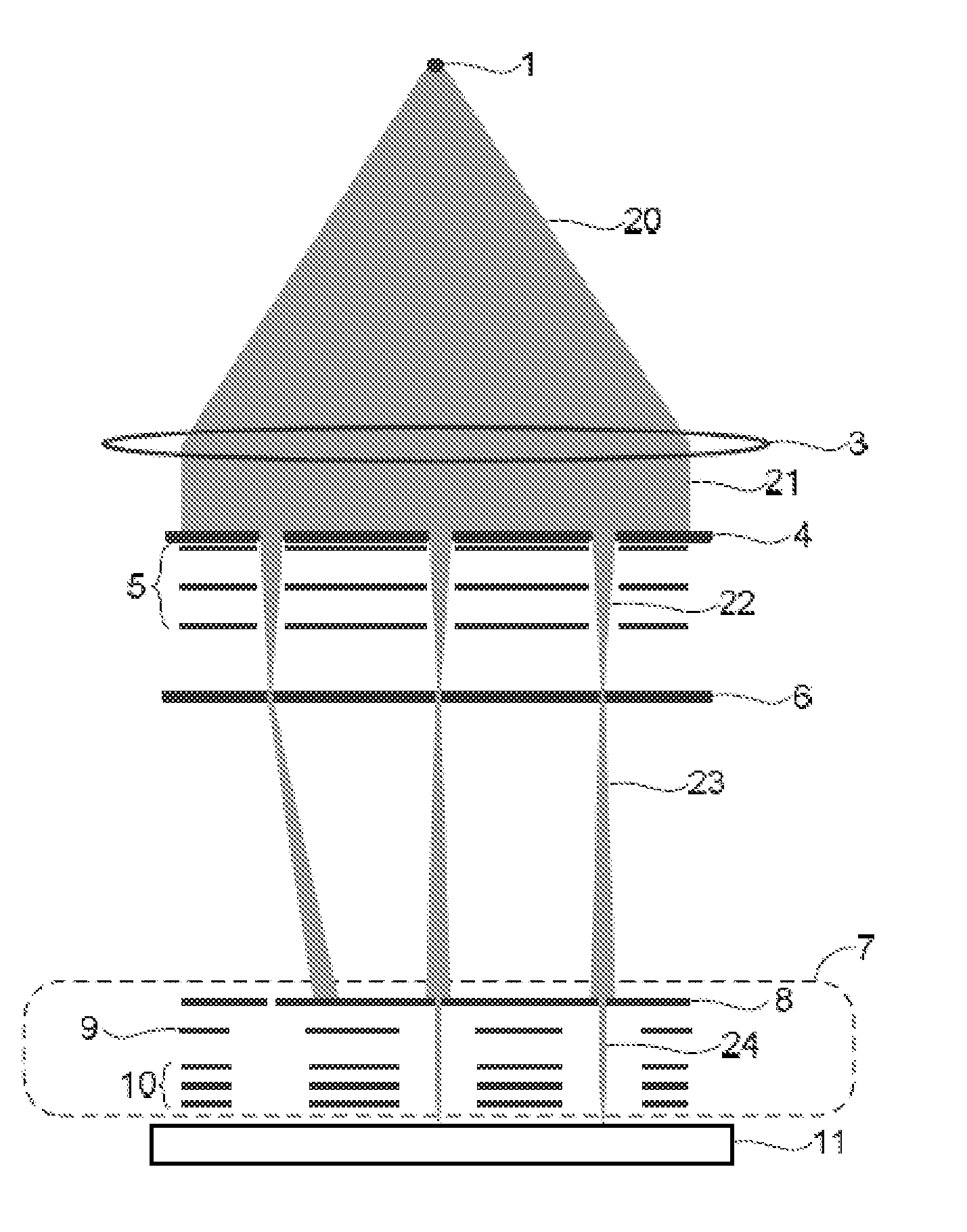
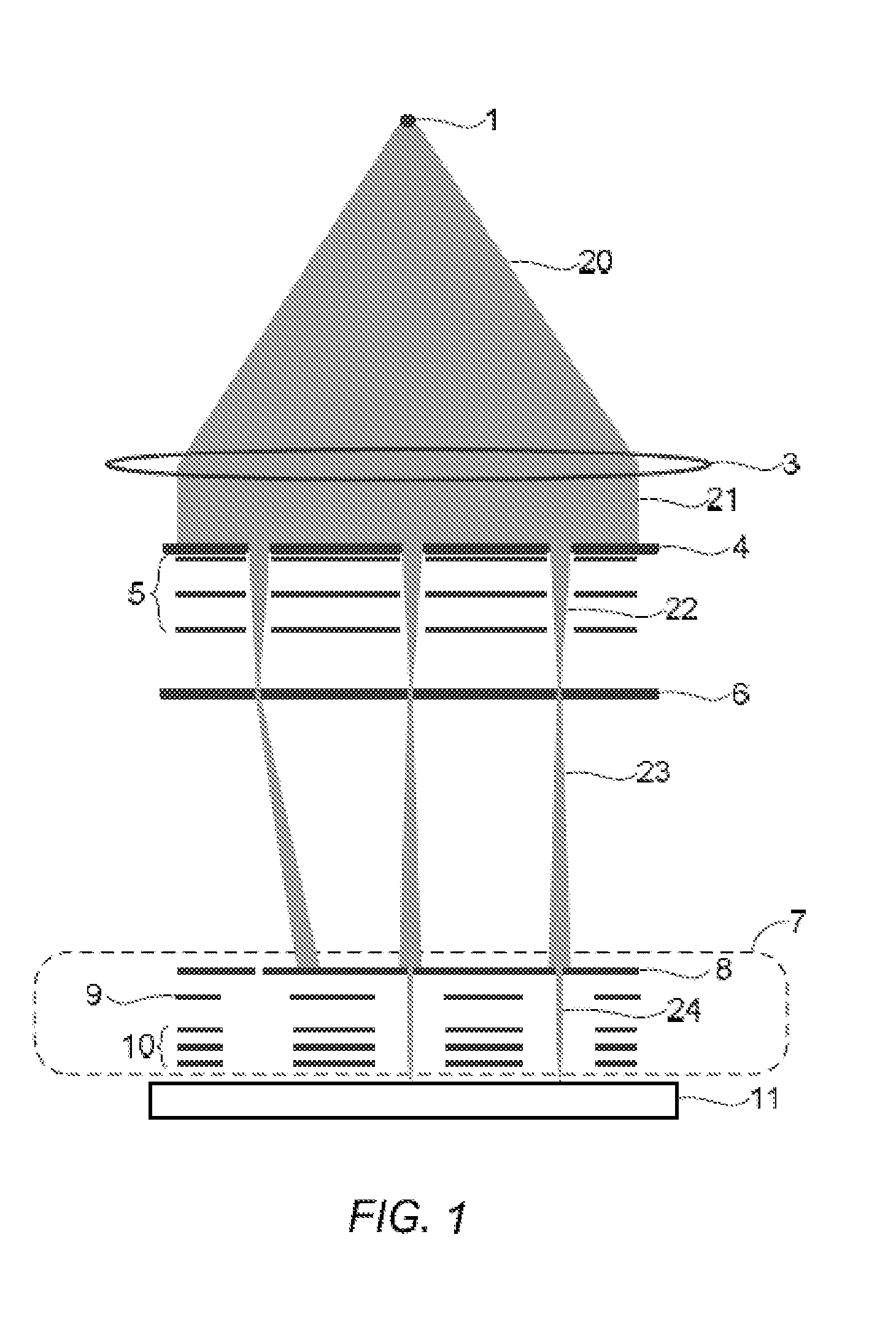
[0024]FIG. 1 shows a simplified schematic drawing of an embodiment of a charged particle multi-beamlet lithography system based upon an electron beam optical system without a common cross-over of all the electron beamlets. Such lithography systems are described for example in U.S. Pat. Nos. 6,897,458 and 6,958,804 and 7,019,908 and 7,084,414 and 7,129,502, U.S. patent application publication no. 2007 / 0064213, and copending U.S. patent applications Ser. Nos. 61 / 031,573 and 61 / 045,243, which are all assigned to the owner of the present invention and are all hereby incorporated by reference in their entirety.

[0025]In the embodiment shown in FIG. 1, the lithography system comprises an electron source 1 for producing a homogeneous, expanding electron beam 20. Note that the electrons will appear to originate from a point above the source, i.e. a vir...


PUM


Abstract

A charged particle multi-beamlet system for exposing a target (11) using a plurality of beamlets. The system comprises a charged particle source (1) for generating a charged particle beam (20), a beamlet aperture array (4D) for defining groups of beamlets (23) from the generated beam, a beamlet blanker array (6) comprising an array of blankers for controllably blanking the beamlets (23), a beam stop array (8) for blanking beamlets (23) deflected by the blankers, the beam stop array (8) comprising an array of apertures, each beam stop aperture corresponding to one or more of the blankers, and an array of projection lens systems (10) for projecting beamlets on to the surface of the target. The system images the source (1) onto a plane at the beam stop array (8), at the effective lens plane of the projection lens systems (10), or between the beam stop array (8) and the effective lens plane of the projection lens systems (10), and the system images the beamlet aperture array (4D) onto the target (11).

Description

BACKGROUND OF THE INVENTION[0001]1. Field of the Invention[0002]The present invention relates to an imaging system, and in particular to a charged particle multi beamlet lithography system or inspection system.[0003]2. Description of the Related Art[0004]Currently, most commercial lithography systems use a mask as a means to store and reproduce the pattern data for exposing a target, such as a wafer with a coating of resist. In a maskless lithography system, beamlets of charged particles are used to write the pattern data onto the target. The beamlets are individually controlled, for example by individually switching them on and off, to generate the required pattern. For high resolution lithography systems designed to operate at a commercially acceptable throughput, the size, complexity, and cost of such systems becomes an obstacle.[0005]One type of design used for charged particle multi-beamlet systems is shown for example in U.S. Pat. No. 5,905,267, in which an electron beam is ex...

Claims


Application Information

Patent Timeline
07 Apr 2011
Publication
US20110079730A1
IPC
H01J3/14
CPC
B82Y10/00; B82Y40/00; H01J2237/0492; H01J2237/0435; H01J37/3177
Inventors
WIELAND, MARCO JAN-JACO