Charge pump circuit, and method of controlling charge pump circuit

a charge pump and circuit technology, applied in the direction of pulse automatic control, dc-dc conversion, power conversion systems, etc., can solve the problems that the negative step-up output voltage cannot be used as a voltage source of electronic devices, remove only noise, etc., and achieve the effect of stabilizing an output voltage and suppressing the generation of nois

Inactive Publication Date: 2011-04-07
PANASONIC CORP
View PDF13 Cites 30 Cited by
  • Summary
  • Abstract
  • Description
  • Claims
  • Application Information

AI Technical Summary

Benefits of technology

[0022]In accordance with the present invention, it is possible to provide a charge pump circuit which is capable of suppressing generation of a noise and stabilizing an output voltage, and a control method thereof.

Problems solved by technology

This causes a problem that the negative step-up output voltage Vout cannot be used as a voltage source of electronic devices such as high-frequency devices which is susceptible to a noise.
For this reason, it is difficult to remove only the noise from the negative step-up output voltage VoutN with a filter for damping a specific frequency region, and the negative step-up output voltage VoutN tends to be a noise source.

Method used


Image

  • Charge pump circuit, and method of controlling charge pump circuit
  • Charge pump circuit, and method of controlling charge pump circuit
  • Charge pump circuit, and method of controlling charge pump circuit

Examples


embodiment 1

Configuration of Charge Pump Circuit

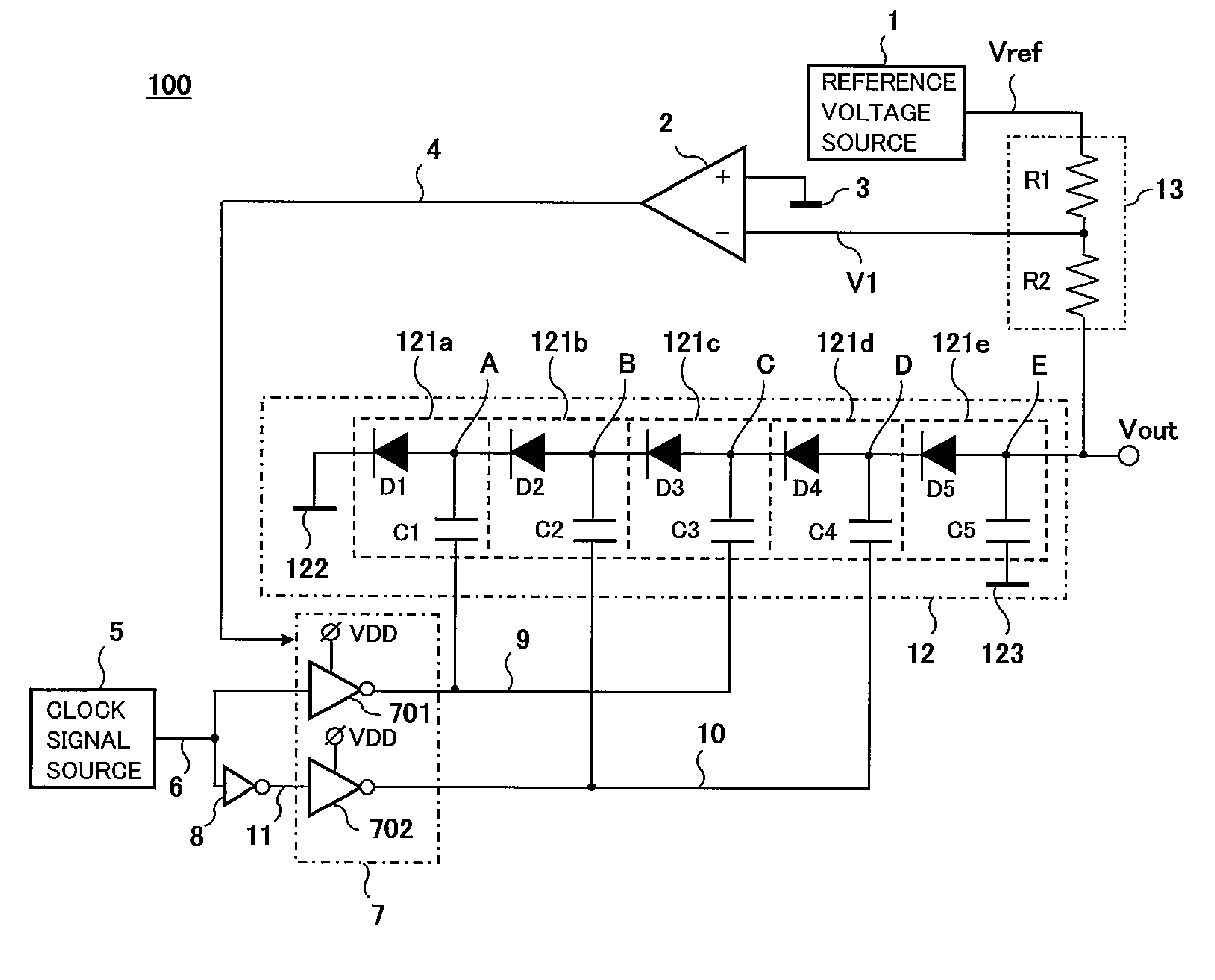
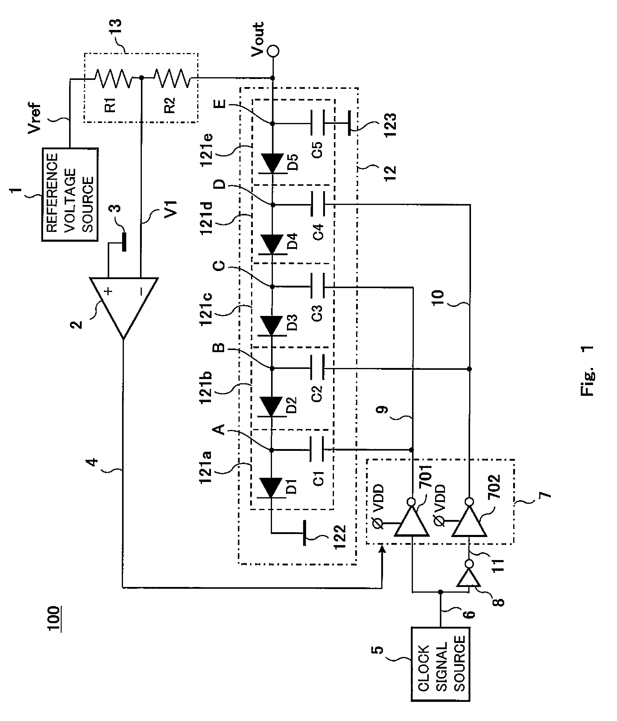
[0033]FIG. 1 is a view showing a configuration of a charge pump circuit according to Embodiment 1 of the present invention. A charge pump circuit 100 of FIG. 1 is configured to output a stable negative step-up output voltage (step-down voltage) Vout through an output terminal Vout.

[0034]The charge pump circuit 100 includes a reference voltage source 1, a differential amplifier 2, a resistance voltage divider 13, a clock signal source 5, a clock feeder 7, a pump circuit section 12 having a Dickson-based configuration, an inverter element 8 and the output terminal Vout.

[0035]The reference voltage source 1 is a voltage source configured to generate and output a reference voltage Vref. As the reference voltage source 1, for example, a band gap reference voltage source (hereinafter BGR (Band Gap Reference)) configured to generate the reference voltage Vref which is less temperature-dependent may be used. The output side of the reference voltage source ...

embodiment 2

Configuration of Clock Feeder

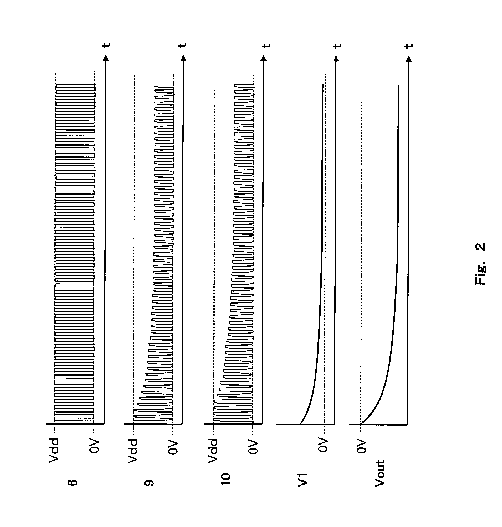
[0093]FIG. 6 shows an exemplary configuration of a clock feeder 7 according to Embodiment 2 of the present invention. With the configuration of the clock feeder 7 of FIG. 6, the advantage similar to that of the clock feeder 7 of FIG. 3 is achieved.

[0094]As shown in FIG. 6, the clock feeder 7 includes the input terminal A, the input terminals CLK1 and CLK2, P-channel MOS transistors M101, M201, M501, and M601, the N-channel MOS transistors M3, M4, M7, and M8, and the output terminals CLKOUT1 and CLKOUT2. The first switching element of the present invention corresponds to the P-channel MOS transistors M201 and M601, while the second switching element of the present invention corresponds to the P-channel MOS transistors M101 and M501 and the N-channel MOS transistors M3 and M7.

[0095]The output signal 4 which is output from the differential amplifier 2 of FIG. 1 is input to the input terminal A. The original clock signal 6 which is output from the clock sign...

embodiment 3

Configuration of Charge Pump Circuit

[0115]As shown in FIG. 7, a charge pump circuit 200 according to Embodiment 3 of the present invention is substantially identical in configuration to the charge pump circuit 100 according to Embodiment 1 of FIG. 1. The charge pump circuit 200 is different in configuration from the charge pump circuit 100 of FIG. 1 in that the reference voltage source 1 of FIG. 1 is replaced by a stabilization voltage source 101 configured to output a constant voltage (e.g., 0V or 4.0V) and the ground terminal 3 is replaced by a negative voltage source 102 configured to output a constant negative voltage (e.g., −1.0V) to the non-inverting input terminal of the differential amplifier 2.

[0116]The stabilization voltage source 101 is configured to output a predetermined reference voltage V2. The reference voltage V2 is applied to the output terminal Vout through the resistance voltage divider 13 including series-coupled resistors R1 and R2.

[0117]The divided voltage por...


PUM


Abstract

A charge pump circuit of the present invention comprises a resistance voltage divider provided between a reference voltage source and an output terminal, a differential amplifier which has an inverting input terminal applied with a divided voltage portion from the resistance voltage divider and a non-inverting input terminal applied with a comparison voltage and is configured to output an output signal obtained by amplifying a potential difference between the divided voltage portion and the comparison voltage through an output terminal, a clock feeder configured to output first and second clock signals according to an original clock signal, and a pump circuit section which is applied with the first and second clock signals alternately and control an output voltage at an output terminal, and the clock feeder is configured to regulate amplitude levels of the first and second clock signals according to the voltage of the output signal.

Description

RELATED APPLICATIONS[0001]The disclosure of Japanese Patent Application No. 2009-230779 filed on Oct. 2, 2009 including specification, drawings and claims is incorporated herein by reference in its entirety.BACKGROUND ART 1. Field of the Invention[0002]The present invention relates to a charge pump circuit which is capable of suppressing generation of a noise and stabilizing an output voltage, and a control method thereof. Particularly, the present invention relates to a charge pump circuit built into electronic devices using high frequencies, and a control method thereof. 2. Description of the Related Art[0003]These days, in some cases, a gate bias of a negative voltage is necessary, when GaAs-FETs are used in semiconductor devices. In these cases, there is a need for a negative step-up circuit (step-down circuit), as a circuit for generating a predetermined negative voltage from a positive power supply voltage. An exemplary negative step-up circuit is configured to include a Dicks...

Claims


Application Information

Patent Timeline
Patent Type & Authority Applications(United States)
IPC IPC(8): H03L7/06
CPCH02M3/073
Inventor OHTA, KAZUYOKIHARA, HIDEYUKI
Owner PANASONIC CORP
Why Eureka
Try Eureka