Programmable antifuse transistor and method for programming thereof

Active Publication Date: 2011-04-07
SILICON LINE
View PDF27 Cites 15 Cited by
  • Summary
  • Abstract
  • Description
  • Claims
  • Application Information

AI Technical Summary

Benefits of technology

[0036]High long-term stability is expected for such areas in the substrate since a voluminous conducting channel can be formed between the drain and the source

Problems solved by technology

As a result of the insulation layer arranged between the two p-type substrates in the form of a deep n-well, additional process steps are required, which complicates production of these known electrically programmable antifuses and incurs higher production costs.
In this instance it has proven to be disadvantageous that no active circuits or active circuit parts can be operated during programming in the vicinity of the antifuse since, as result of the increased substrate potential, the function of active circuit(s)/circuit part(s) of this type is at least limited, or else they may even no longer be operational.
Alternatively or in addition, the prior art also poses the risk that a parasitic thyristor may be ignited by increasing the substrate potenti

Method used


Image

  • Programmable antifuse transistor and method for programming thereof
  • Programmable antifuse transistor and method for programming thereof
  • Programmable antifuse transistor and method for programming thereof

Examples


Embodiment Construction

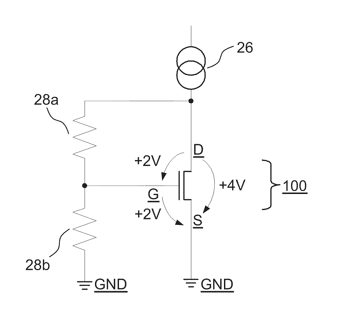
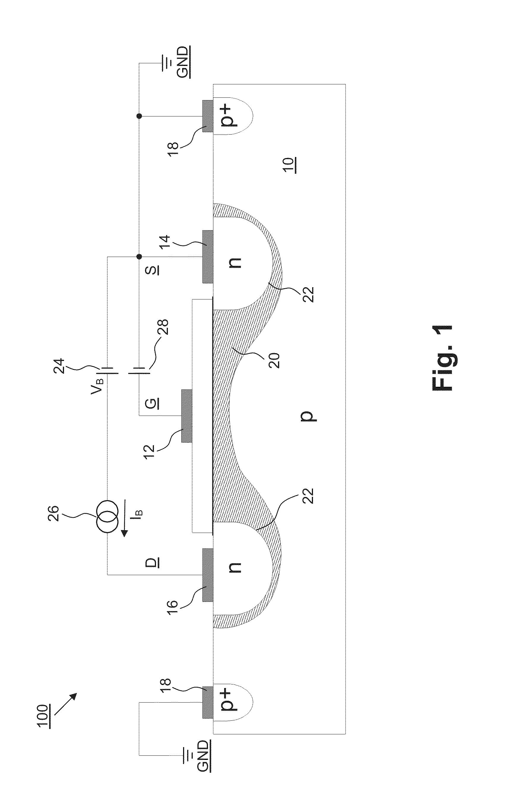
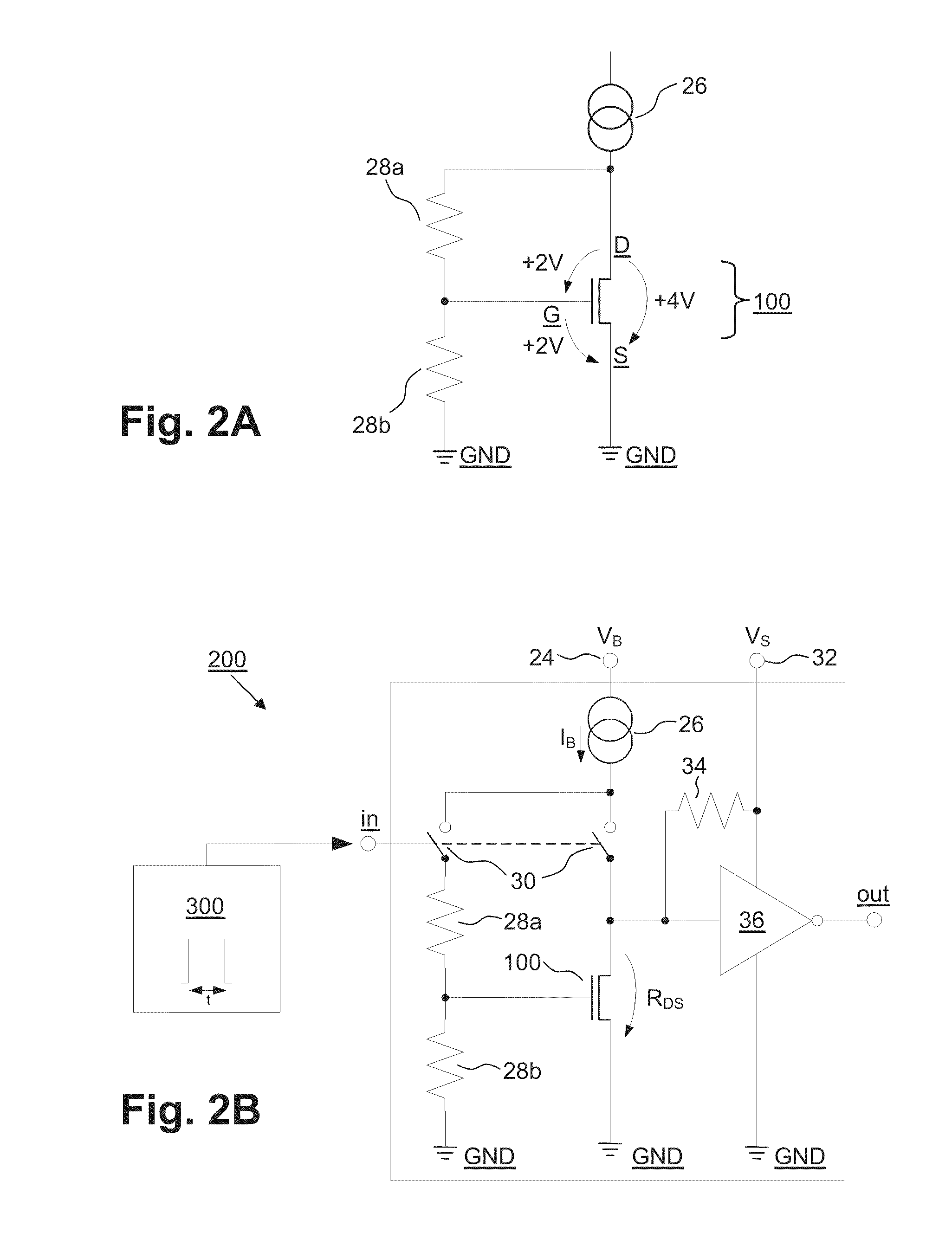
[0045]FIG. 1 shows a schematic cross-sectional view of an embodiment of a programmable antifuse n-channel MOS transistor 100 according to the present invention that operates by the method according to the present invention and the conductivity of which in the programmed state is about 10,000 times greater than in the unprogrammed state.

[0046]The antifuse transistor 100 comprises

[0047]a gate G with terminal (=gate contact or gate terminal) 12,

[0048]a source S with terminal (=source contact or source terminal) 14,

[0049]a drain D with terminal (=drain contact or drain terminal) 16 and

[0050]a substrate 10 with terminal (=substrate contact or substrate terminal) 18

(the source S corresponds to an emitter; the drain D corresponds to a collector; the substrate 10 corresponds to a base).

[0051]The level of the potential difference between the source terminal 14 and the substrate terminal 18 is generally selected to be smaller than the forward voltage of silicon pn junctions 22 arranged in a c...


PUM


Abstract

Programmable antifuse transistor, in particular n-channel MOS transistor, and a method for programming at least one such antifuse transistor, includes at least one gate with a gate terminal, source with a source terminal, drain with a drain terminal, and substrate with a substrate terminal, configured so that active circuits/circuit elements do not have to be located at a distance from the antifuse, minimizing area requirements, without additional process steps the level of the potential difference between source terminal and substrate terminal is less than about 0.5 volts, drain terminal and source terminal lie at different potentials. By adjusting drain-source voltage and/or the gate-source voltage a flow of charge carriers occurs between source and drain, causing semiconductor material between source and drain to be thermally heated and to locally melt, forming at least one permanently conducting channel between source and drain.

Description

CROSS-REFERENCE TO RELATED APPLICATIONS[0001]This application is a continuation of application no. PCT / EP2009 / 054483, filed 16 Apr. 2009, which claims the priority of German application no. 10 2008 001 217.3, filed 16 Apr. 2008, and which application no. PCT / EP2009 / 054483, filed 16 Apr. 2009, claims the priority of German application no. 10 2009 001 923.5, filed 26 Mar. 2009, and each of which is incorporated herein by reference.FIELD OF THE INVENTION[0002]The present invention relates to a programmable antifuse transistor. More particularly, the present invention relates to a programmable antifuse transistor, in particular an n-channel MOS transistor. The present invention further relates to an antifuse circuit arrangement, in particular a one-time electrically programmable permanent storage cell. The present invention further relates to an antifuse circuit arrangement of this type which may be configured as an area-efficient, one-time electrically programmable permanent storage ce...

Claims


Application Information

Patent Timeline
IPC IPC(8): G11C17/16H01L23/525
CPCG11C17/16G11C17/18H01L2924/0002H01L2924/00
Inventor GROEPL, MARTINHOELTKE, HOLGER
Owner SILICON LINE
Why Eureka
Try Eureka