Power amplifier

a power amplifier and power technology, applied in the field of amplifiers, can solve the problems of low breakdown voltage, relatively high cost and better features of gaas process, and large loss of silicon substrate, and achieve the effect of improving the efficiency of the power amplifier

Active Publication Date: 2011-04-21
IND TECH RES INST
View PDF6 Cites 12 Cited by
  • Summary
  • Abstract
  • Description
  • Claims
  • Application Information

AI Technical Summary

Benefits of technology

[0008]In an exemplary embodiment, there is provided a power amplifier, in which the gate bias of the power amplifier is dynamically adjusted according to an input power, so as to improve an efficiency of the power amplifier through adaptive bias.
[0010]According to the above description, in the exemplary embodiment, the power detector is used to detect the input power of the amplifier, and then the bias control circuit adjusts the gate bias of the amplifier according to the input power of the amplifier, so as to improve the efficiency of the power amplifier. Moreover, according to a feature that a drain current of a field-effect transistor (FET) is in inverse proportion to temperature while amplifier is biased in class A manner, the quiescent current of power amplifier was reduced when operated temperature was increase. This feature generate a reduction of the gain which aggravate the linearity. By using the characteristic that the drain current of FET is in direct proportion to temperature while its gate bias is near the threshold voltage, the gain reduction of the amplifier operated in high temperature is compensated. Therefore, the power amplifier of the present invention has advantages of temperature compensation and linearity improvement.

Problems solved by technology

However, to achieve a strict device specification for most of the communication systems, in a radio frequency (RF) circuit, besides the RF transceiver is implemented by the CMOS process, key components (for example, a power amplifier and a transceiver switch) of the front end RF circuit are all fabricated by a GaAs process with relatively high cost and better features due to a relatively great loss of the silicon substrate.
Compared to a conventional power amplifier of the GaAs process, disadvantages of a conventional power amplifier of the silicon process include low breakdown voltage, high loss of the silicon substrate and none backside via structure.
Therefore, implementation of impedance matching of the output terminal can lead to a relatively great loss especially on the substrate with higher silicon process loss.
Therefore, the power amplifier known to a person of skill in the art implemented by the silicon process has lower efficiency, and remained energy is converted into heat and accumulated in the substrate.
Moreover, none backside via structure is provided during the CMOS process, so that in case of signal grounding of the amplifier of a common source structure, a bond wire has to be used to connect a printed circuit board or a package outside the chip, which may prolong the signal grounding path, and a parasitic inductance effect can severely influence the efficiency of the power amplifier.
To resolve the above problem, a method known to a person of skill in the art is to add a DC-to-DC converter in the circuit or provide a reference voltage through the system, though both circuit structures thereof are complicated, which is of no avail for SoC implementation.

Method used


Image

  • Power amplifier
  • Power amplifier
  • Power amplifier

Examples


Embodiment Construction

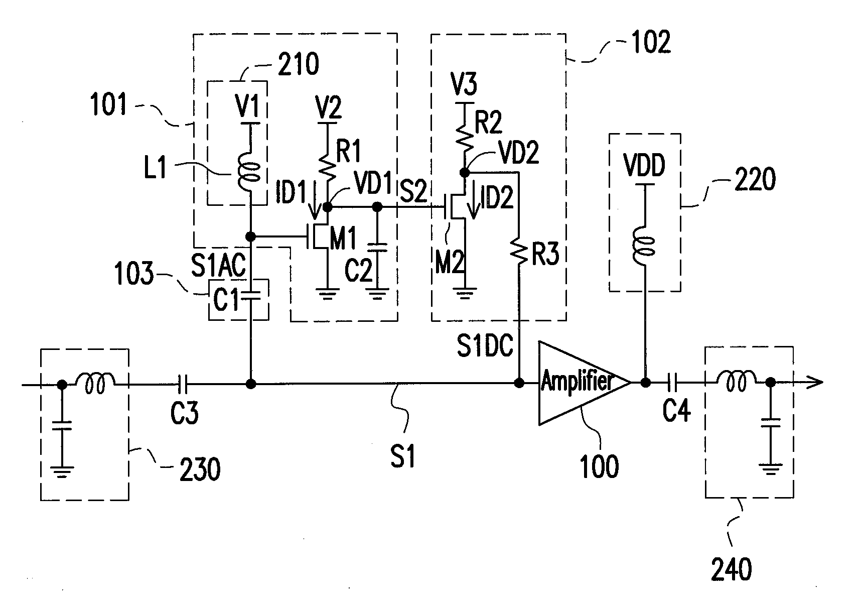
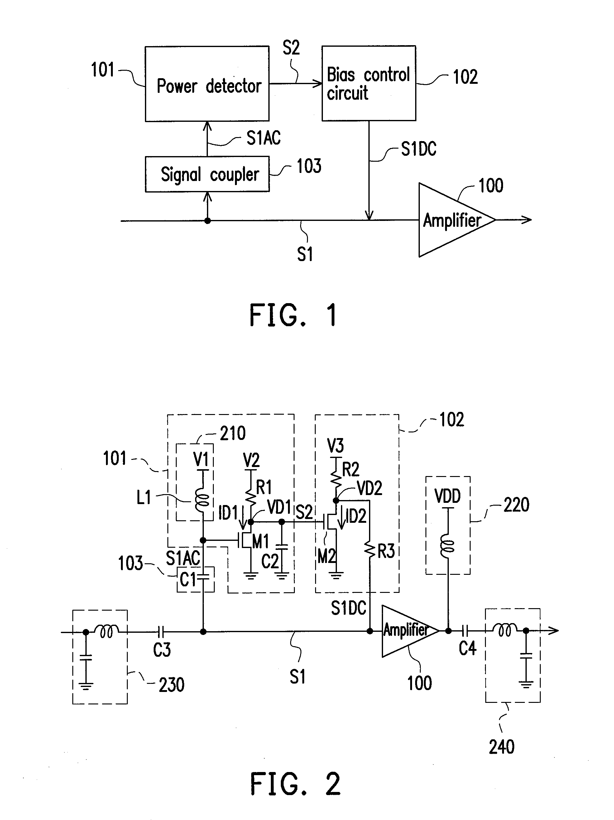
[0017]A direct current (DC) bias of a power amplifier known to a person of skill in the art is fixed. During the operation of the power amplifier known to a person of skill in the art, the fixed bias leads to a fixed DC power consumption, so that when the power amplifier known to a person of skill in the art is operated in a low power region, an efficiency of the power amplifier is greatly reduced. Namely, most of the DC electric energy is converted into heat to increase an operation temperature. The high operation temperature influences a characteristic of the power amplifier. To mitigate the shortcoming of low efficiency of the power amplifier operated in the low power region, according to a method known to a person of skill in the art, the DC bias of the amplifier is design to have a low bias value. Such method can effectively reduce the DC power consumption of the amplifier to improve the efficiency. However, when the power amplifier is operated in a high power region, the low D...


PUM


Abstract

An adaptive bias power amplifier including an amplifier, a signal coupler, a power detector and a bias control circuit is provided. The signal coupler is connected to an input terminal of the amplifier. The power detector is connected to the signal coupler, and detects an input power of the amplifier via the signal coupler. The bias control circuit is connected to an output terminal of the power detector and the input terminal of the amplifier. The bias control circuit adjusts a gate bias of the amplifier in accordance with a detecting result of the power detector.

Description

CROSS-REFERENCE TO RELATED APPLICATION[0001]This application claims the priority benefit of U.S. provisional application Ser. No. 61 / 253,061, filed on Oct. 19, 2009. The entirety of the above-mentioned patent application is hereby incorporated by reference herein and made a part of specification.BACKGROUND OF THE INVENTION[0002]1. Technical Field[0003]The disclosure relates to an amplifier.[0004]2. Description of Related Art[0005]Silicon process techniques such as complementary metal-oxide semiconductor (CMOS) and SiGe have been widely and successfully used in wireless communication electronic circuits. Besides cost and size are considered, a main characteristic of the silicon process technique that various digital and analogic circuits can be integrated in a same process, so as to achieve a purpose of system-on-chip (SoC). However, to achieve a strict device specification for most of the communication systems, in a radio frequency (RF) circuit, besides the RF transceiver is impleme...

Claims


Application Information

Patent Timeline
Patent Type & Authority Applications(United States)
IPC IPC(8): H03F3/04
CPCH03F1/0266H03F2200/18H03F2200/105
Inventor CHANG, DE-CHENGHSU, YU-CHENG
Owner IND TECH RES INST
Why Eureka
Try Eureka