

Organic electroluminescent display device and method of fabricating the same
- Summary
- Abstract
- Description
- Claims
- Application Information
AI Technical Summary
Benefits of technology
Problems solved by technology
Method used
Image

Examples
first embodiment
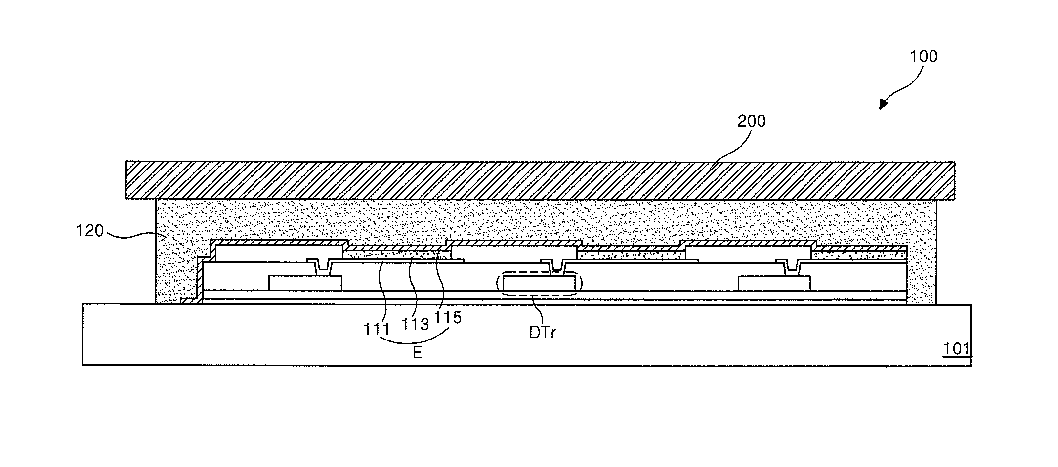
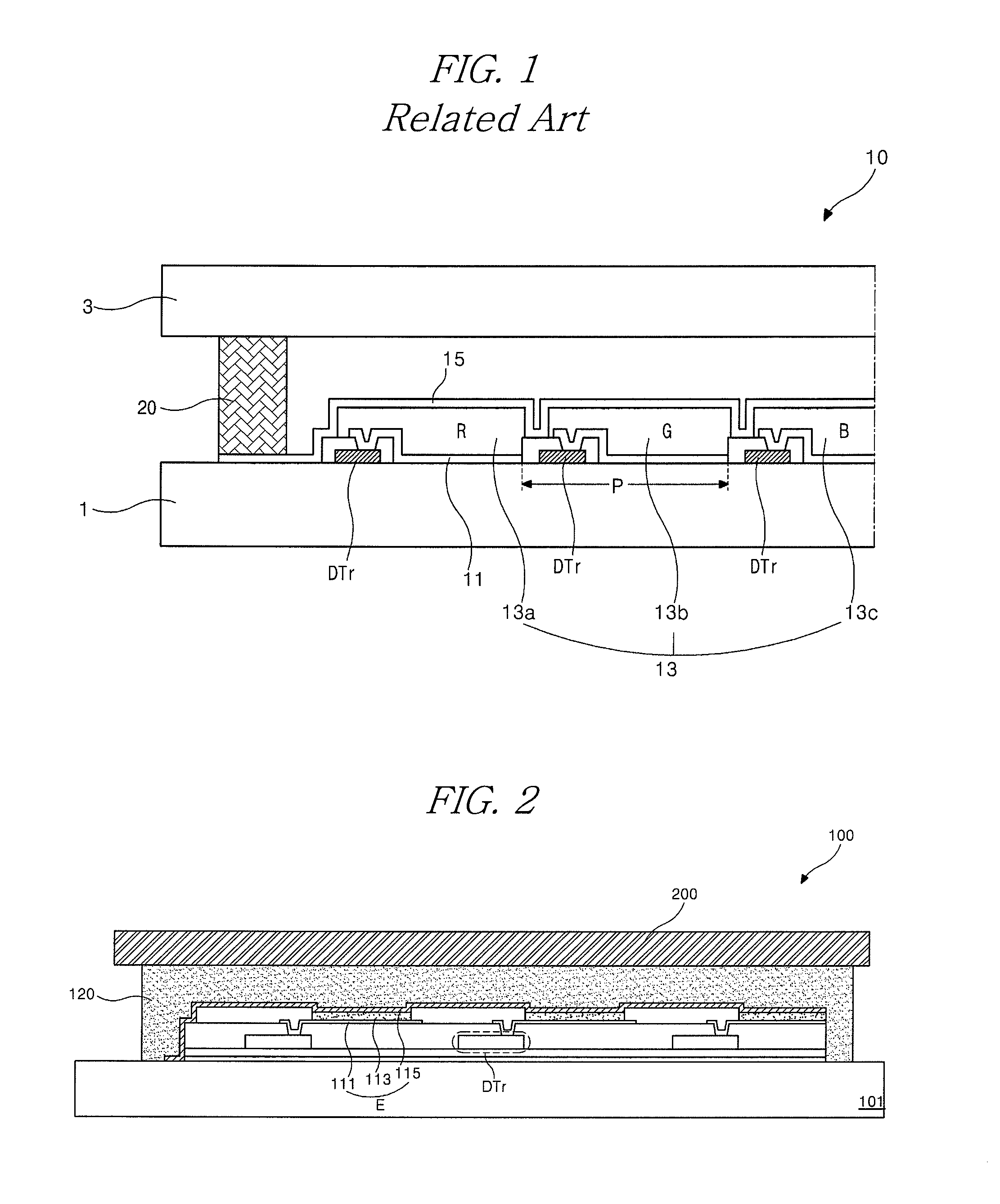
FIG. 2 is a cross-sectional view showing an organic electroluminescent display device of a bottom emission type according to the present invention.
In FIG. 2, the organic electroluminescent display (ELD) device 100 includes an array substrate 101 where a driving thin film transistor (TFT) DTr, a switching TFT (not shown) and an organic electroluminescent (EL) diode E are formed thereon and a metal foil 200. The driving TFT DTr is formed in each pixel region P on the array substrate 101, and the organic EL diode E includes a first electrode 111 connected to the driving TFT DTr, an organic luminescent layer 113 emitting a colored light on the first electrode 111 and a second electrode 115 on the organic luminescent layer 113. In the organic ELD device 100, the first and second electrodes 111 and 115 function as an anode and a cathode, respectively.
The metal foil 200 is formed over the driving TFT DTr and the organic EL diode E. The array substrate 101 and the metal foil 200 are attache...
second embodiment
FIGS. 4A to 4H are cross-sectional views showing a fabrication process for an organic electroluminescent display device according to the present invention.
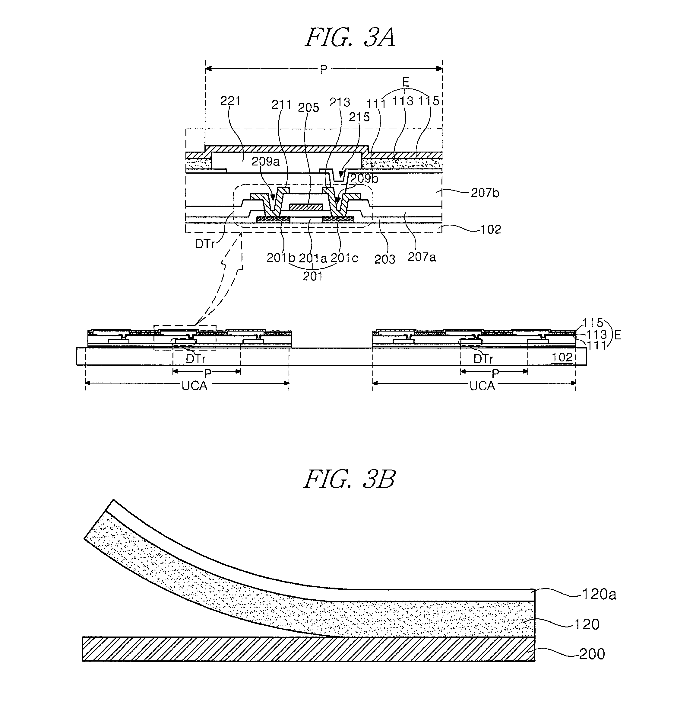
In FIG. 4A, a mother substrate 102 includes a plurality of unit cell areas UCA, and a switching thin film transistor (TFT) (not shown), a driving TFT DTr and an organic electroluminescent (EL) diode E are formed in each unit cell area UCA of the mother substrate 102. The mother substrate 102 may include a glass or a transparent plastic. Each unit cell area UCA includes a plurality of pixel regions P. The mother substrate 102 is cut in a subsequent process to become a plurality of array substrates 101 (of FIG. 4H), and each of the plurality of array substrates 101 constitutes an organic electroluminescent display (ELD) device 100 (of FIG. 4H).
After an amorphous silicon layer (not shown) is formed in each pixel region P on the mother substrate 102 by depositing amorphous silicon, the amorphous silicon layer is crystallized by a lase...
PUM
 Abstract
Description
Claims
Application Information