Forming a Photovoltaic Device

Inactive Publication Date: 2011-05-12
IBM CORP
View PDF4 Cites 32 Cited by
  • Summary
  • Abstract
  • Description
  • Claims
  • Application Information

AI Technical Summary

Benefits of technology

[0011]Aspects of the invention provide, for example, a low-cost method for forming thin film photovoltaic materials, such as thin film photovoltaic material used in solar cells. Principles of the invention provide, for example, chemical processes for incorporating gallium into

Problems solved by technology

Crystalline silicon solar cells have a relatively high efficiency for conver

Method used


Image

  • Forming a Photovoltaic Device
  • Forming a Photovoltaic Device
  • Forming a Photovoltaic Device

Examples


Embodiment Construction

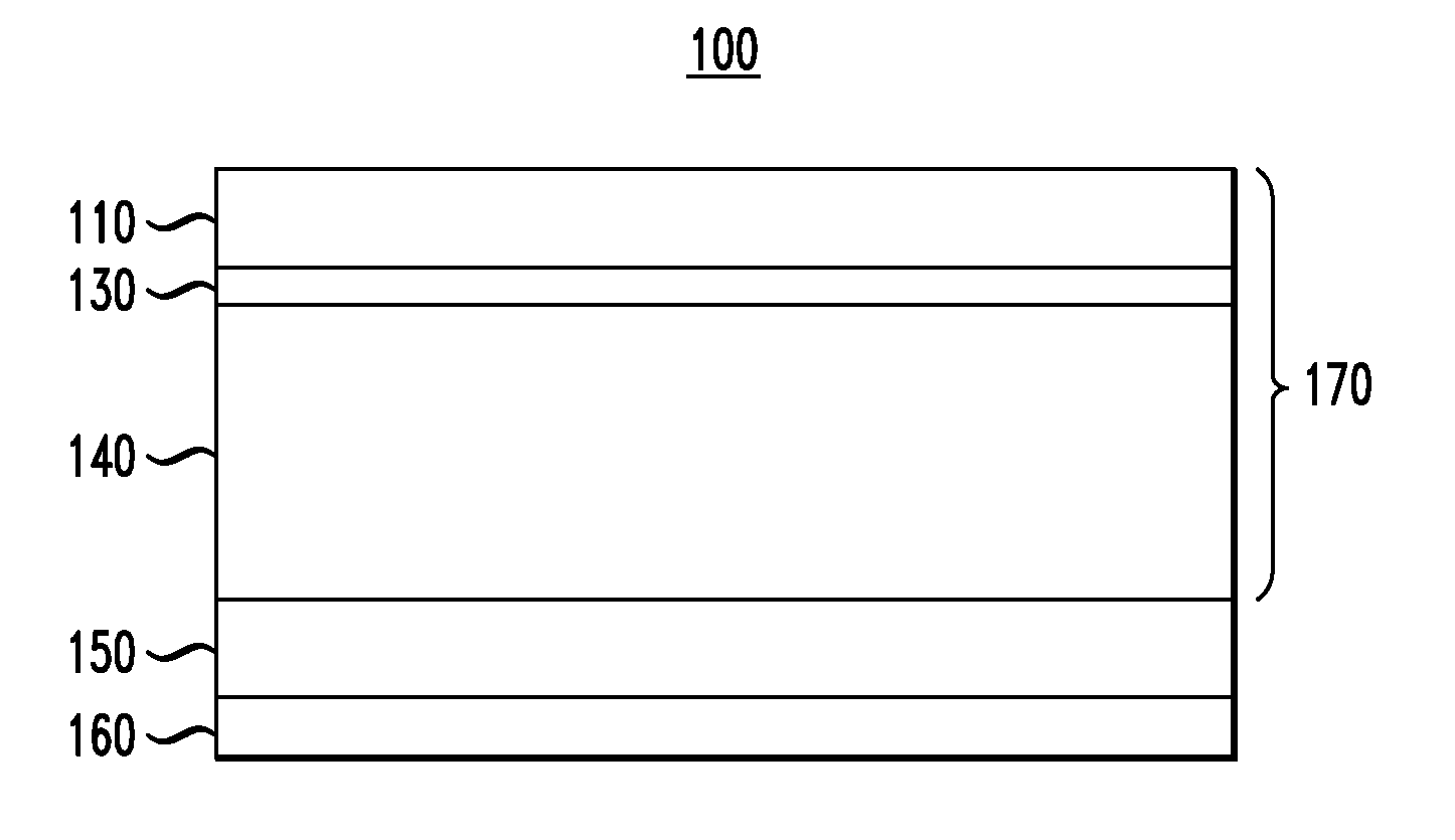
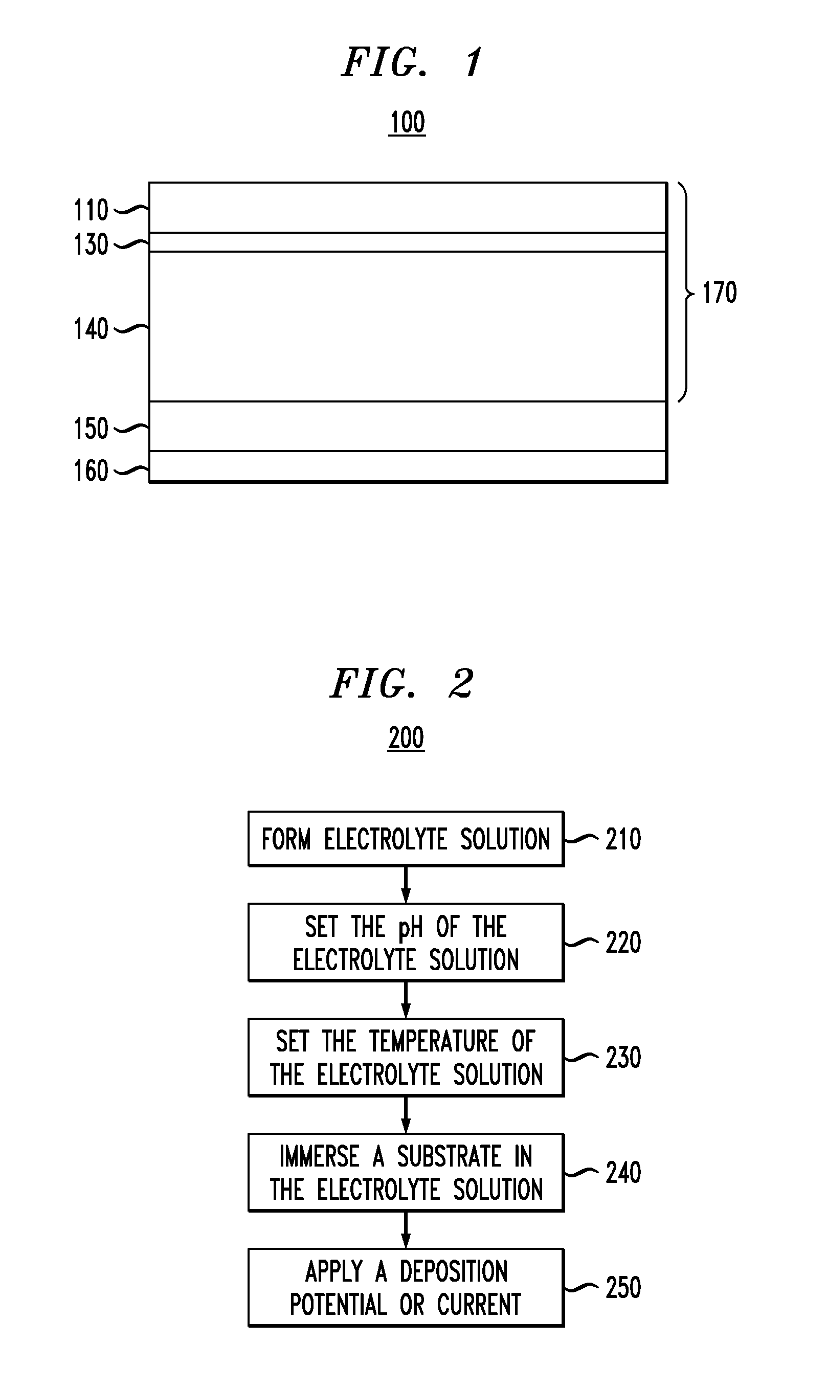
[0016]Principles of the present invention will be described herein in the context of illustrative methods for forming solar cells and semiconductor compounds. It is to be appreciated, however, that the techniques of the present invention are not limited to the specific method and devices shown and described herein. Rather, embodiments of the invention are directed broadly to techniques for electrodeposition of semiconductors and devices formed by the electrodeposition of the semiconductors. For this reason, numerous modifications can be made to the embodiments shown that are within the scope of the present invention. No limitations with respect to the specific embodiments described herein are intended or should be inferred.

[0017]Electrodeposition is a process of depositing one or more materials onto one or more substrate materials using electrical current. Electrodeposition processes include, for example, electroplating and electrophoretic deposition. For example, electrodeposition ...


PUM

PropertyMeasurementUnit
Temperatureaaaaaaaaaa
Fractionaaaaaaaaaa
Electric potential / voltageaaaaaaaaaa

Abstract

Methods for forming photovoltaic devices, methods for forming semiconductor compounds, photovoltaic device and chemical solutions are presented. For example, a method for forming a photovoltaic device comprising a semiconductor layer includes forming the semiconductor layer by electrodeposition from an electrolyte solution. The electrolyte solution includes copper, indium, gallium, selenous acid (H2SeO3) and water.

Description

FIELD OF THE INVENTION[0001]The present invention relates generally to photovoltaic devices formed by electrodeposition, and more particularly the invention relates to solar cells formed by electrodeposition of semiconductor compounds.BACKGROUND OF THE INVENTION[0002]Electrodeposition can be used for relatively low cost deposition of thin film materials for photovoltaic applications. Cadmium telluride, copper indium di-selenide and copper indium gallium di-selenide are such materials and are used to make solar cells. Electrodeposition involves depositing from a solution, using electrical current, of a material onto a substrate. Electroplating and electrophoretic deposition are types of electrodeposition.[0003]Solar cells convert light energy, such as sunlight, into electrical energy. One type of solar cell is fabricated from bulk or crystalline silicon. Crystalline silicon solar cells have a relatively high efficiency for conversion of light into electricity, but are relatively expe...

Claims


Application Information

Patent Timeline
IPC IPC(8): H01L31/0296H01L31/18
CPCC25D3/56Y02E10/541H01L31/18H01L31/0322
Inventor DELIGIANNI, HARIKLIAROMANKIW, LUBOMYR T.VAIDYANATHAN, RAMAN
Owner IBM CORP
Why Eureka
Try Eureka