
Paper-based microfluidic systems

Active Publication Date: 2011-05-12
PRESIDENT & FELLOWS OF HARVARD COLLEGE
View PDF91 Cites 97 Cited by
  • Summary
  • Abstract
  • Description
  • Claims
  • Application Information

AI Technical Summary

Benefits of technology

[0031]In other embodiments, the method further comprises applying an electric charge to a second strip of conductive material, wherein applying the electric current to the second strip of conductive material prevents the fluidic flow of the sample from a second minor channel region to a second assay region.

Problems solved by technology

Most current bioanalytical assays are inaccessible for developing economies.
Current diagnostic assays typically require large and expensive laboratory instruments that are operated by trained personnel.

Method used


Image

  • Paper-based microfluidic systems
  • Paper-based microfluidic systems
  • Paper-based microfluidic systems

Examples


example 1

Preparation and Use of Paper Microfluidic Device for Analyte Concentration

[0102]Fabricating a Paper Microfluidic Device

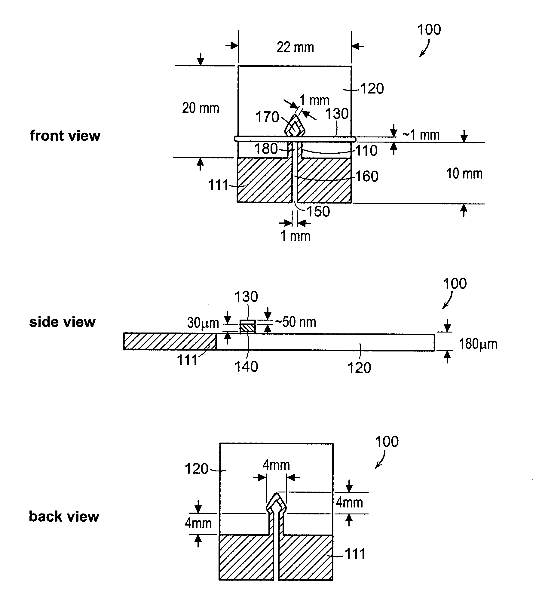
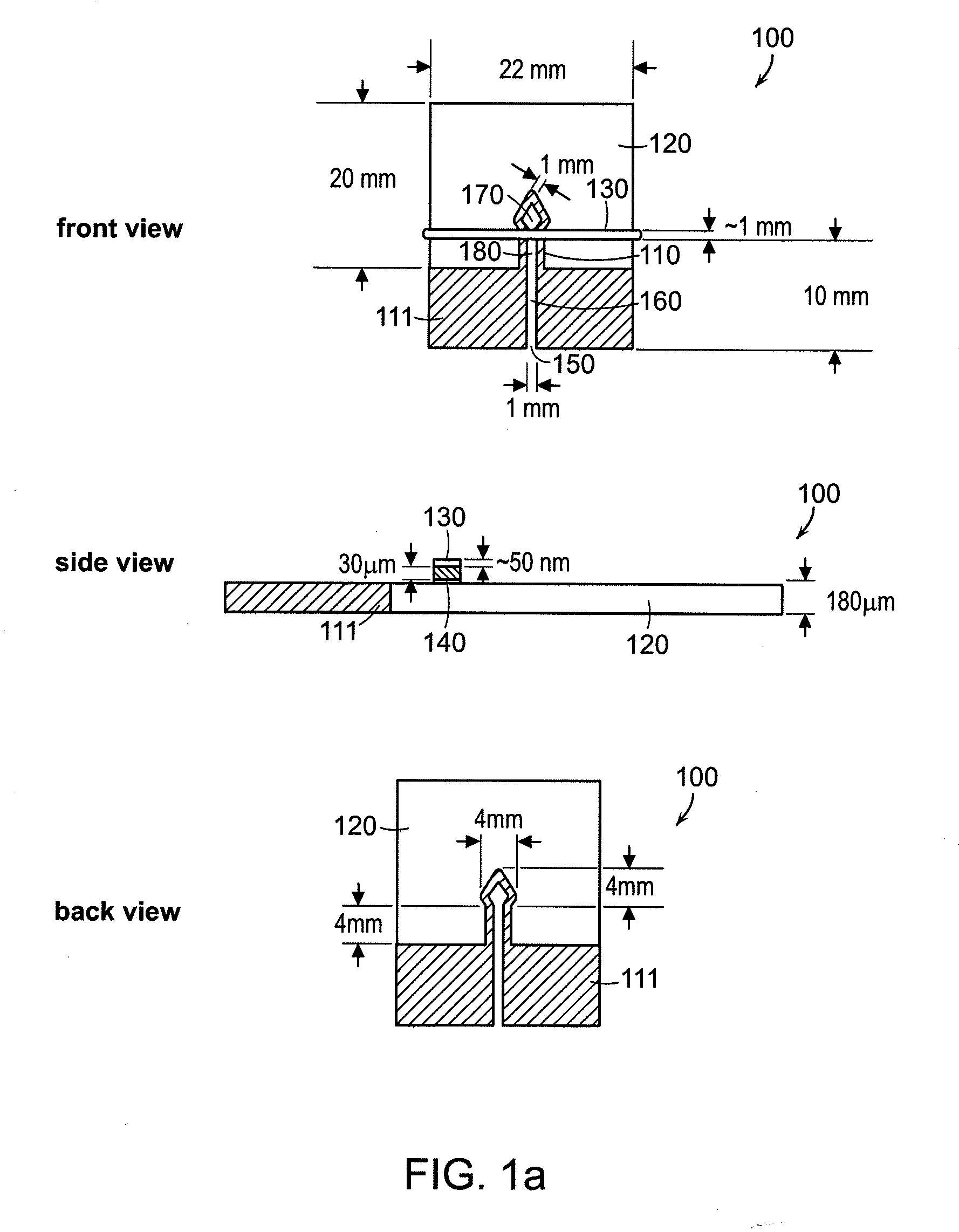
[0103]The prototype μ-PADs was fabricated in a two step process (see FIG. 2). The μ-PADs were prepared in a two-step process that involved creating patterns of hydrophobic polymer in paper, and patterning conductive gold pathways onto the paper-based microfluidic devices.

[0104]First, the microfluidic channels were formed in Whatman filter paper 1 using photolithography and SU-8 photoresist, as described previously (Martinez et al., Angew. Chem. Int. Ed., Eng. 46:1318-1320, 2007). Briefly, this process involved embedding SU-8 photoresist into Whatman filter paper 1, drying the paper to remove the cyclopentanone in the SU-8 formula, and then irradiating the paper for around 3.5 min (using a 100 W mercury lamp) through a pattern of black ink printed onto a transparency. The paper was heated at 90° C. for 10 min, soaked in propylene glycol methyl ether acetate (3×5 min)...

example 2

Preparation and Use of Paper Microfluidic Device for Detecting Salt Concentration

[0114]Fabricating a Paper Microfluidic Device

[0115]Microfluidic channels were fabricated in filter paper (Whatman, Inc.) using a process described previously (Martinez et al., Angew. Chem. Int. Ed., Eng. 6:1318-1320,2007) (see FIG. 5). The patterns for the microfluidic channels were designed on a computer using a layout editor (Clewin, WieWin Inc.) and a photomask was printed from the design using an inkjet printer and a transparency film. The microfluidic channels were patterned in Whatman filter paper 1 using the following process: (i) paper (2.5 cm×2.5 cm×200 μm) was soaked in resist (SU-8 2010, Microchem Inc.), and a rolling pin was used to press excess resist from the paper; (ii) the paper was dried for 10 min at 95° C., the photomask was clamped to the paper by pressing them together as a sandwich between two glass slides that were held together with binder clips, and the paper was exposed to UV l...

example 3

Preparation and Use of Paper Microfluidic Device with Switches and Valves

[0128]Fabrication of the Devices

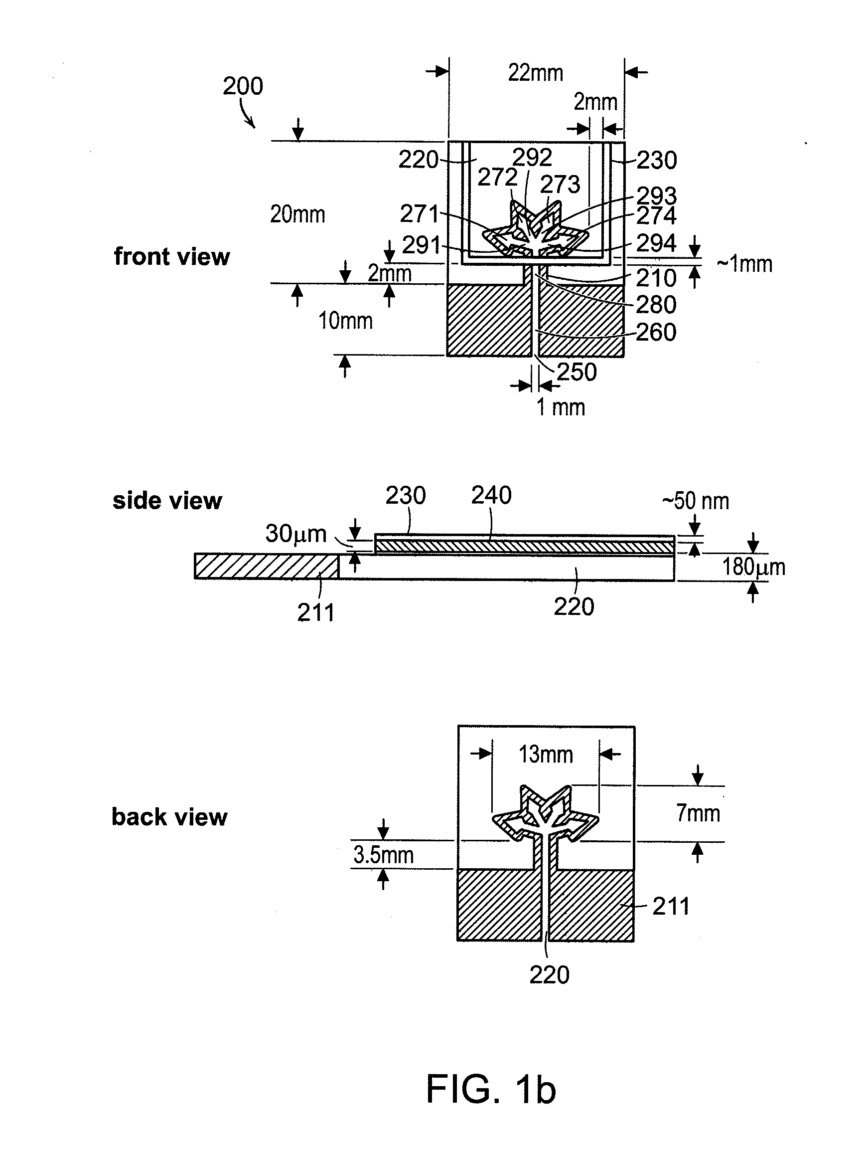
[0129]The microfluidic devices were fabricated using a process that consisted of three general steps: (i) photolithography on a Whatman filter paper 1 using SU-8 photoresist, according to product specifications (MicroChem Corp., Newton, Mass.); (ii) fabrication and attachment of metal-tape wires: 50 nm layer of gold was sputtered (Cressington Model 208HR sputter coater, 60 mA, 50 s sputtering time) onto a matt side of the Scotch tape and attached to the device as a 1-mm-wide strip; and (iii) assembling all the layers of the device.

[0130]Switching the Channels On / Off

[0131]To investigate the switching on / off process in the paper channel, an aqueous solution of red dye (0.05 mM aq. disodium 6-hydroxy-5-((2-methoxy-5-methyl-4-sulfophenyl)azo)-2-naphthalene-sulfonate, allura red) was used to visualize the effectiveness of the device. The solution was conveyed to the central channel of...


PUM


Abstract

Paper-based microfluidic systems and methods of making the same are described.

Description

CROSS-REFERENCE TO RELATED APPLICATIONS[0001]This application claims the benefit of U.S. Provisional Application No. 61 / 039,858, filed Mar. 27, 2008, and U.S. Provisional Application No. 61 / 039,958, filed Mar. 27, 2008, the contents of which are hereby incorporated in their entirety herein.BACKGROUND OF THE INVENTION[0002]Most current bioanalytical assays are inaccessible for developing economies. Current diagnostic assays typically require large and expensive laboratory instruments that are operated by trained personnel. Thus, there remains a need for low-cost diagnostic assays that are not cumbersome and that can be performed on small sample volumes. Further, there remains a need for low-cost systems to detect trace levels of analytes in fluids for, e.g., (i) human health; (ii) illicit drug use; (iii) military and homeland security settings; and (iv) chemical pollution in the environment.SUMMARY OF THE INVENTION[0003]In one aspect, the invention features an assay device. The assay...

Claims


Application Information

Patent Timeline
IPC IPC(8): G01N21/00C12M1/34G01N21/75
CPCB01L3/502707Y10T436/2575B01L2200/0642B01L2200/10B01L2200/12B01L2200/16B01L2300/025B01L2300/0636B01L2300/0645B01L2300/0809B01L2300/0819B01L2300/087B01L2300/12B01L2300/161B01L2300/1827Y10T436/25B01L2200/027B01L2400/0406B01L2300/126
Inventor SIEGEL, ADAM C.PHILLIPS, SCOTT T.DICKEY, MICHAEL D.ROZKIEWICZ, DOROTAWILEY, BENJAMINWHITESIDES, GEORGE M.MARTINEZ, ANDRES W.
Owner PRESIDENT & FELLOWS OF HARVARD COLLEGE
Learn More