Acceleration sensor and method of fabricating acceleration sensor

a sensor and acceleration technology, applied in the direction of acceleration measurement in multiple dimensions, acceleration measurement using interia forces, instruments, etc., can solve the problems of change in characteristics, external stress to the sensor chip cannot be completely blocked, and the sensor chip cannot be completely shattered, so as to prevent the penetration of sealing resin inside the frame portion, the effect of excellent strength and shock resistan

Active Publication Date: 2011-05-19
LAPIS SEMICON CO LTD
View PDF1 Cites 19 Cited by
  • Summary
  • Abstract
  • Description
  • Claims
  • Application Information

AI Technical Summary

Benefits of technology

[0035]In the invention of the above configuration, a configuration can be achieved with excellent strength and shock resistance by employing the glass substrate.
[0036]A fifth aspect of the present invention provides the acceleration sensor of the first aspect, wherein an outside of the frame portion is sealed with a sealing resin, and a sealing frame is provided to each of the frame portion and the lid portion to prevent the sealing resin from penetrating inside the frame portion.
[0037]In the invention of the above configuration, a configuration can be achieved in which penetration of the sealing resin inside the frame portion is prevented by providing the sealing frames to the frame portion and the lid portion and by sealing the outside of the frame portion with the sealing resin.

Problems solved by technology

However, with the structure described in Document 1 above, while the stress to the acceleration sensor from outside is cushioned by the silicon plate, and influence on the sensor characteristics are suppressed, after substrate mounting, external stress from a direction along the substrate surface cannot be completely blocked from the detection portion of the sensor, and a concern exists that stress will cause a change in characteristics.
Furthermore, in the configuration of the fifth exemplary embodiment described in JP-A No. 2008-026183 above, FIG. 5, there is an SOIC package configured from a metal plate (bottom plate) and sealing resin, and since the sealing resin covers the outside of a support body, there is a concern that stress from the sealing resin is transmitted to the support body or a beam portion, with the possibility that stress might cause a change in characteristics of the sensor.
Furthermore, in the structure described in JP-A No. 2000-187040, a groove is provided cut into the rear face of the support portion as a stress relief portion, however the structure is such that external stress to the sensor chip cannot be completely blocked from the flexible portion by the cut in groove, and there is a concern that the external stress will cause a change in characteristics.

Method used


Image

  • Acceleration sensor and method of fabricating acceleration sensor
  • Acceleration sensor and method of fabricating acceleration sensor
  • Acceleration sensor and method of fabricating acceleration sensor

Examples


second exemplary embodiment

[0153]FIGS. 5A and 5B, and FIGS. 6A and 6B show a structure of an acceleration sensor according to a second exemplary embodiment of the present invention. An acceleration sensor 101 according to the second exemplary embodiment of the present invention is in the form of a package, called a WCSP, indicating a package in which redistribution wiring, protection film, and terminals are formed while in the wafer state, for subsequent conversion into individual chips.

[0154]In the WCSP, the mounting surface area of the package is the same size as that of the semiconductor chip itself, there is no requirement for installation to a lead-frame, and there is the merit of being more compact than the first exemplary embodiment in which molding, with resin or the like, and forming the terminals is performed after the wafer has been converted into individual chips. Furthermore, due to connecting the bonding pads directly, rather than indirectly, to the substrate with Cu posts (solder balls) provide...

third exemplary embodiment

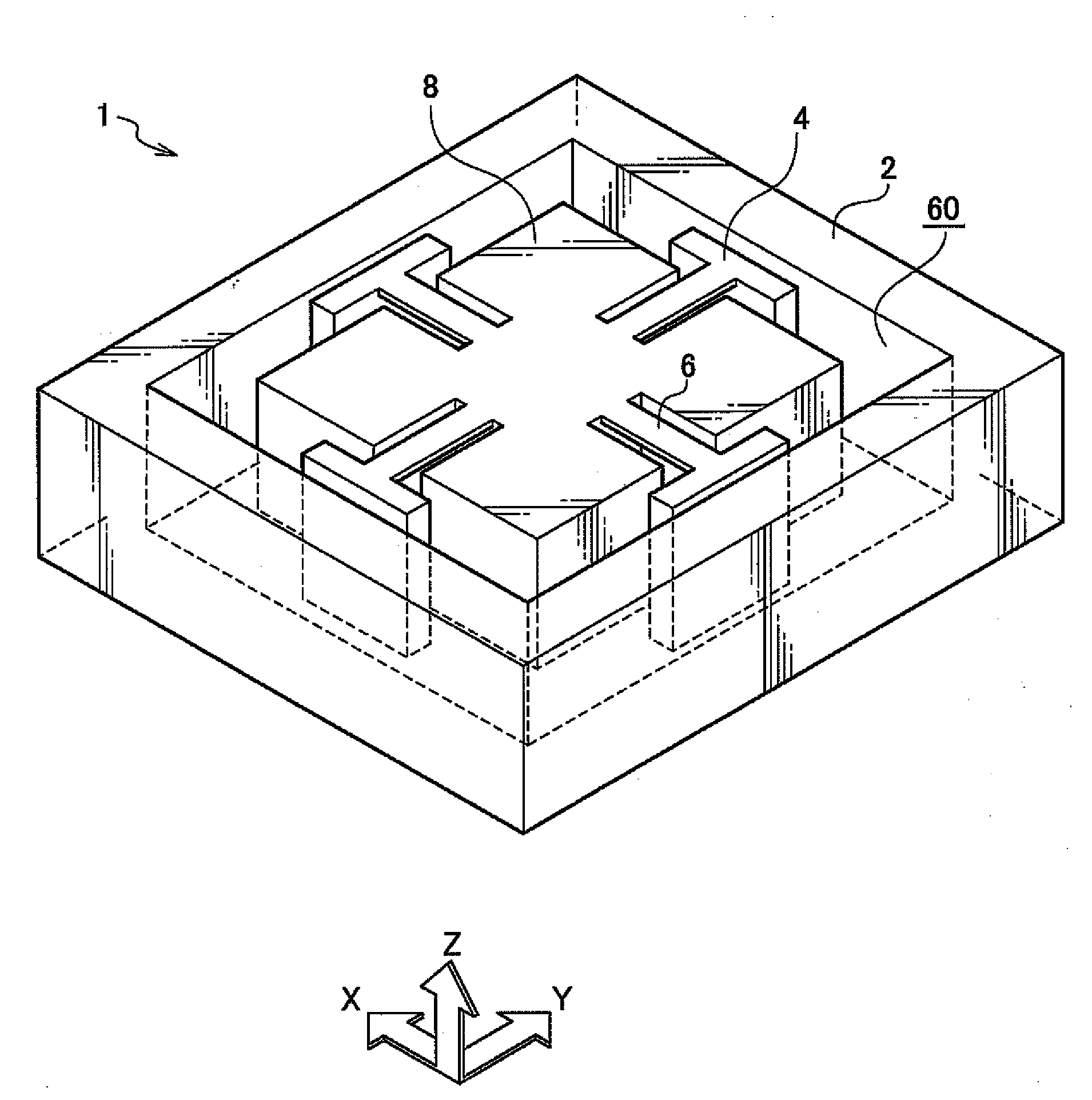
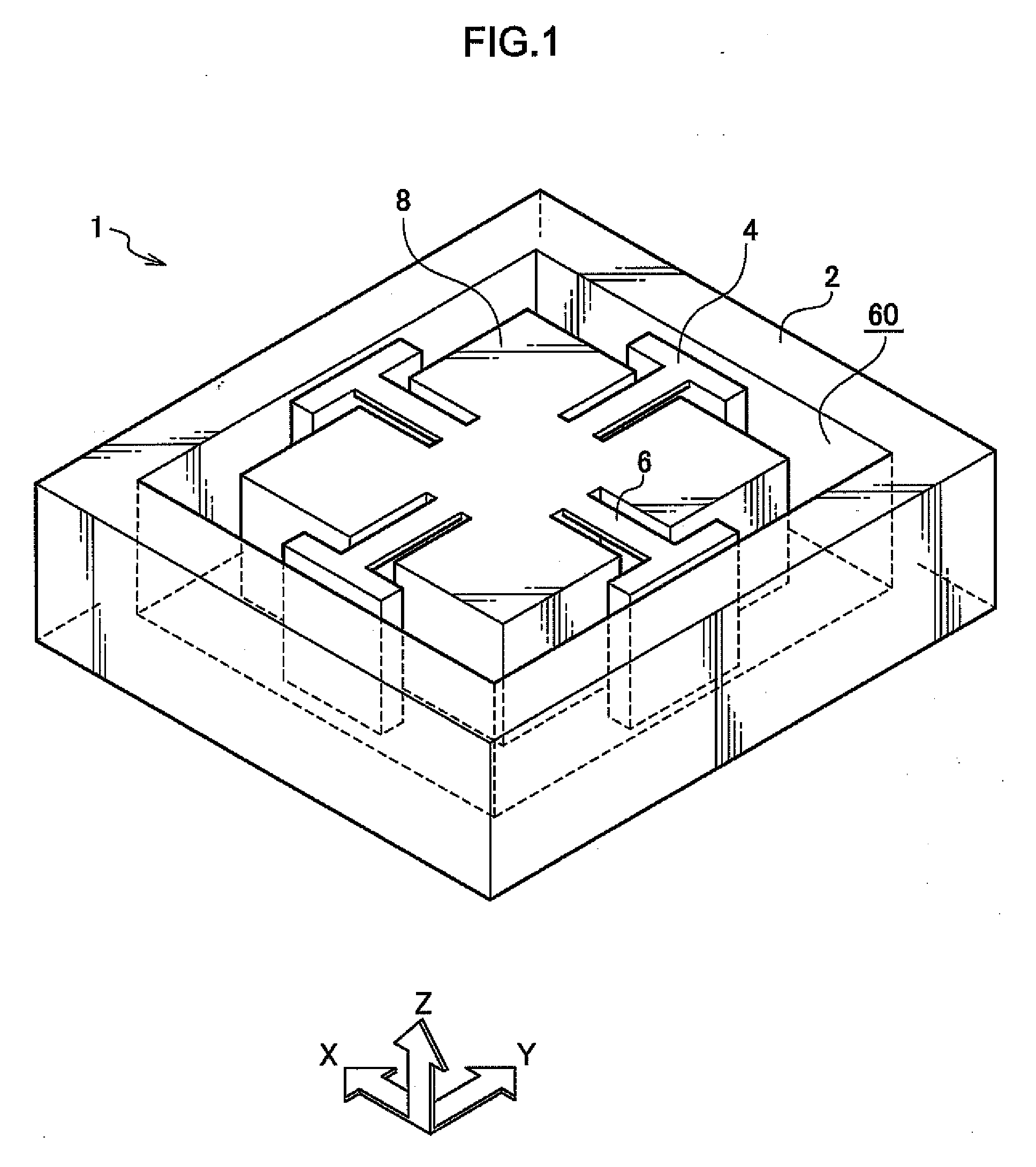
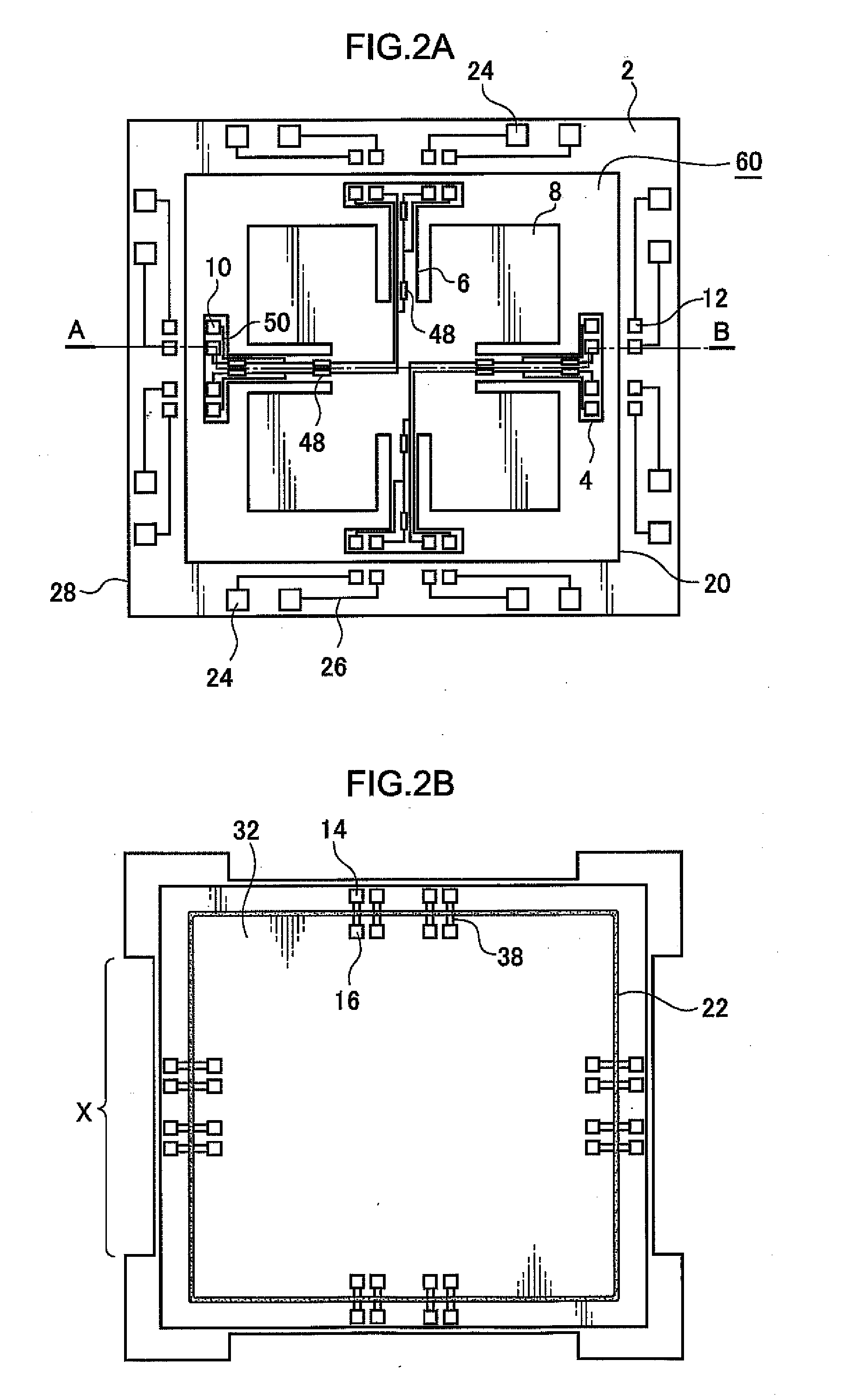
[0173]FIG. 7A and FIG. 7B show a structure of an acceleration sensor according to a third exemplary embodiment of the present invention. As shown in FIG. 7A and FIG. 7B, an acceleration sensor 102 according to the third exemplary embodiment of the present invention, similarly to in the first exemplary embodiment, is connected by the wiring 26 from the external-frame-top connection pads 12, which are electrically connected to the piezoresistor 48 provided to the beams 6, to the bonding pads 24 provided on the external frame 2.

[0174]Since the bonding pads 24 and the wiring 26 to the bonding pads 24 here on the external frame 2 can be placed as desired, configuration may be made such that, as shown in FIG. 7A, the bonding pads 24 are concentrated together.

[0175]In this configuration, by disposing the bonding pads 24 so as to be concentrated along an edge at one side of the acceleration sensor 102, wiring connection can be performed from a single edge, and since wiring is no longer requ...


PUM

PropertyMeasurementUnit
thicknessaaaaaaaaaa
thicknessaaaaaaaaaa
thicknessaaaaaaaaaa

Abstract

There is provided an acceleration sensor including: a weight portion; plural fixed portions formed above a bottom plate around a periphery of the weight portion; a beam portion coupling the fixed portions and the weight portion, and holding the weight portion at a position separated from the bottom plate; a detection portion provided at the beam portion and detecting deformation of the beam portion; a frame portion provided so as to project out from the bottom plate and surround the fixed portions at a position separated from the fixed portions; and a lid portion of plate shape that seals an opening of the frame portion.

Description

CROSS-REFERENCE TO RELATED APPLICATION[0001]This application is based on and claims priority under 35 USC 119 from Japanese Patent Application No. 2009-262104 filed on Nov. 17, 2009, the disclosure of which is incorporated by reference herein.BACKGROUND[0002]1. Technical Field[0003]The present invention relates to an acceleration sensor and to a method of fabricating an acceleration sensor.[0004]2. Related Art[0005]Wafer-Level Chip Size Packages (WCSP) and plastic packages are effective as a way to realize more compact and lower cost electrical components, including ICs.[0006]For example, in Document 1, G Li and A A Tseng, Low stress packaging of a miromachined accelerometer, IEEE Transactions on Electronics Packaging Manufacturing, Vol. 24, pp 18-25, January 2001, a configuration is described in which an acceleration sensor is sealed on a plate produced from silicon, and covered over with a gel. The acceleration sensor is cushioned from external stress by the gel and the silicon pl...

Claims


Application Information

Patent Timeline
Patent Type & Authority Applications(United States)
IPC IPC(8): G01P15/00H05K13/00B26D3/00G01P15/08G01P15/12G01P15/18H01L29/84
CPCG01P15/0802Y10T29/49002G01P15/18G01P15/123G01P2015/0842Y10T83/04
Inventor SUZUKI, TAKEHARU
Owner LAPIS SEMICON CO LTD
Why Eureka
Try Eureka