Compound material, method of producing the same and apparatus for producing the same

a technology of compound material and method, which is applied in the direction of liquid/solution decomposition chemical coating, transportation and packaging, coatings, etc., can solve the problems of poor adhesion of silicon with a plated metal, insufficient adhesive of metal or the like formed by plating as described above, etc., to achieve precise filling of pores, improve adhesion, and less voids

Inactive Publication Date: 2011-05-19
JAPAN SCI & TECH CORP
View PDF16 Cites 9 Cited by
  • Summary
  • Abstract
  • Description
  • Claims
  • Application Information

AI Technical Summary

Benefits of technology

[0032]With use of a composite material according to the present invention, a method of producing a composite material according to the present invention, or an apparatus for producing a composite material according to the present invention, non-penetrating pores formed in a silicon surface layer are filled up with a metal or an alloy of the metal with less voids being left. As a result, because of the advantageous effect of precise filling in the pores, it is possible to improve the adhesion between the silicon surface and a film or a layer of a second metal or an alloy of the second metal, which is formed on the silicon surface other than inside the pores subsequently to the filling in the pores.

Problems solved by technology

However, such a film of a metal or the like to be formed by plating as described above is not sufficiently adhesive to the matrix unless the matrix is appropriately selected.
However, as having been pointed out, silicon generally has poor adhesion with a plated metal (Patent Document 1, for example).

Method used


Image

  • Compound material, method of producing the same and apparatus for producing the same
  • Compound material, method of producing the same and apparatus for producing the same
  • Compound material, method of producing the same and apparatus for producing the same

Examples


first embodiment

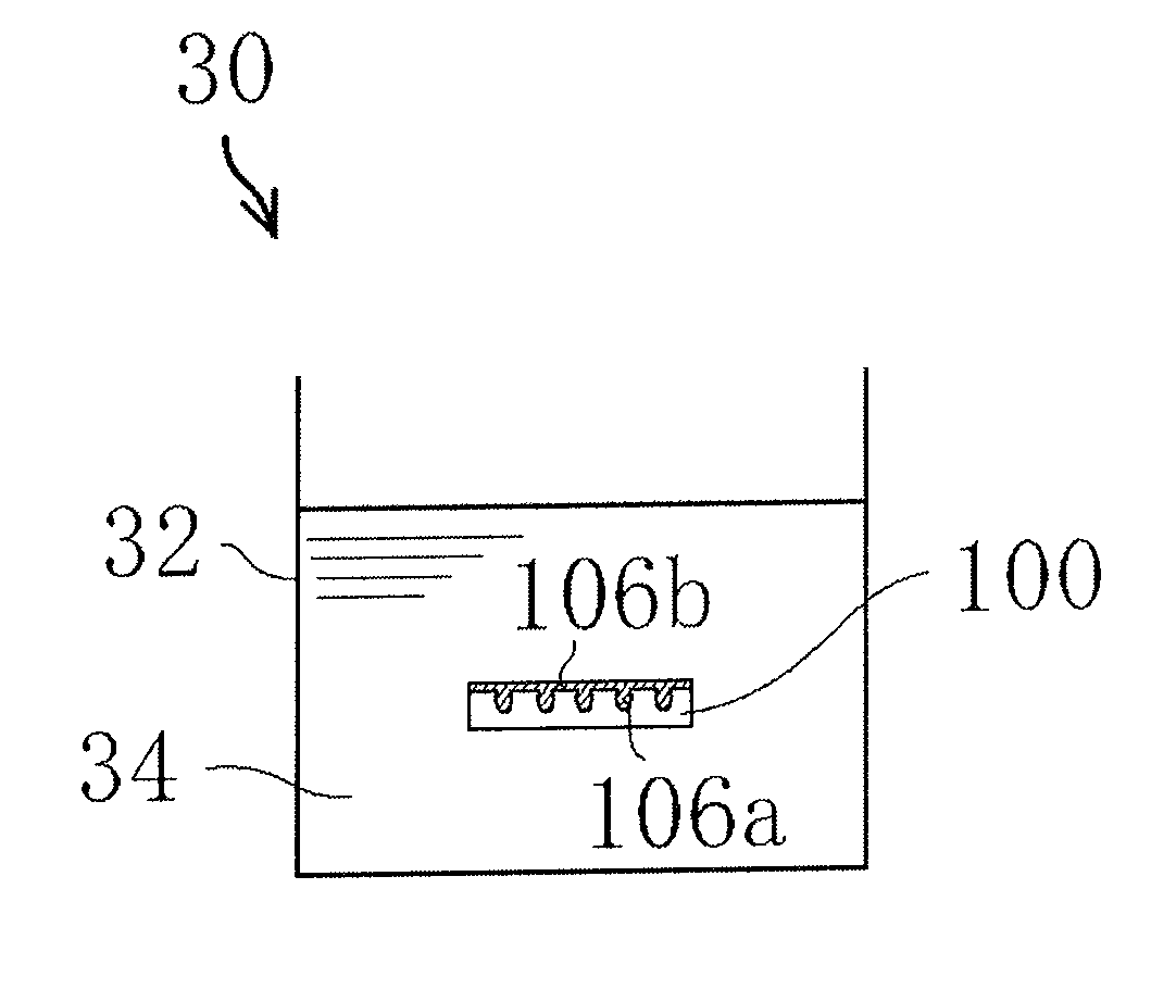
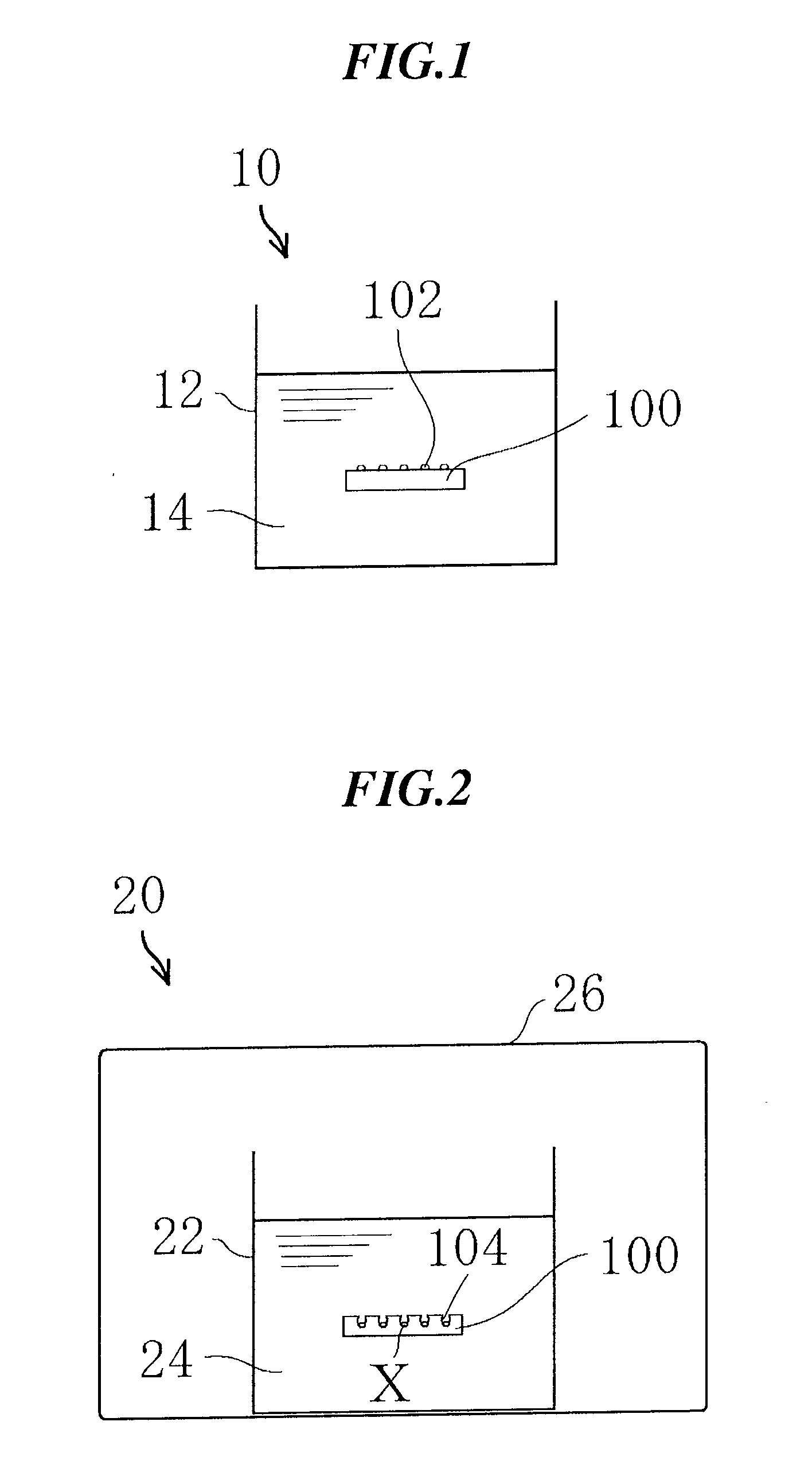
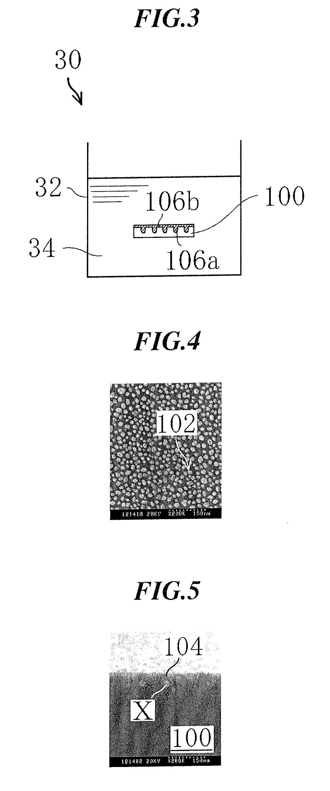
[0047]Described in the present embodiment are a composite material and a method of producing the same. FIG. 1 is a diagram illustrating a dispersion / allocation device 10 for dispersing and allocating a first metal on a surface of a silicon substrate 100, which serves as a matrix, according to the present embodiment. FIG. 2 is a diagram illustrating a non-penetrating pore forming device 20 for forming non-penetrating pores in the surface of the silicon substrate 100. FIG. 3 is a diagram illustrating a plating device 30 for filling in the non-penetrating pores a second metal or an alloy of the second metal and forming on the surface of the silicon substrate 100 a film or a layer of the second metal or an alloy of the second metal (hereinafter, selectively referred to as a “layer” for the purpose of easier description). The present embodiment adopts silver (Ag) as the first metal and cobalt (Co) as the second metal or an alloy of the second metal.

[0048]As shown in FIG. 1, in the presen...

second embodiment

[0060]Described in the present embodiment are another composite material and a method of producing the same. The method of producing the composite material according to the present embodiment is same as that of the first embodiment except for some conditions. Therefore, the description redundant with that of the first embodiment may not be repeatedly provided. A first metal 102 in the present embodiment is dispersed and allocated into the shapes of particles or islands when a silicon substrate is immersed in a first solution 14. However, in the present embodiment, such shapes are selectively referred to as “particles” for the purpose of easier description.

[0061]In the present embodiment, particles of silver (Ag) as the first metal 102 were dispersed and allocated on the surface of a silicon substrate 100, which serves as a matrix, with use of a dispersion / allocation device 10 configured as shown in FIG. 1. More specifically, the present embodiment adopts as the first solution 14 an ...

third embodiment

[0069]Described in the present embodiment are a different composite material and a method of producing the same. The method of producing the composite material according to the present embodiment is same as that of the first embodiment except for the matrix thereof. Therefore, the description redundant with that of the first embodiment may not be repeatedly provided. A first metal 302 in the present embodiment is dispersed and allocated into the shapes of particles or islands when the matrix is immersed in a first solution 14. However, in the present embodiment, such shapes are selectively referred to as “particles” for the purpose of easier description.

[0070]The present embodiment adopts a polycrystalline silicon substrate 300 as a matrix thereof. Again in the present embodiment, the first metal 302 of silver (Ag) was dispersed and allocated on the surface of the polycrystalline silicon substrate, which serves as the matrix, with use of a dispersion / allocation device 10 configured ...


PUM

PropertyMeasurementUnit
diametersaaaaaaaaaa
thickaaaaaaaaaa
depthaaaaaaaaaa

Abstract

Proposed are a composite material having a high adhesiveness, wherein non-penetrating pores that are formed in a silicone surface layer are filled up with a metal or the like without leaving any voids by using the plating technique and the silicone surface layer is coated with the metal or the like, and a method of producing the composite material. A composite material, which has a high adhesiveness between a second metal or an alloy of the second metal (106a, 106b) and a silicone surface, can be obtained by filling up non-penetrating pores that are formed in the surface of a silicone substrate (100) substantially with a second metal or an alloy of the second metal (106a) with the use of the autocatalytic electroless plating technique wherein a first metal located at the bottom of the non-penetrating pores as described above serves as the starting point, and coating the surface of the silicone substrate (100) with the second metal (106b).

Description

TECHNICAL FIELD[0001]The present invention relates to a composite material, a method of producing the same, and an apparatus for producing the same.BACKGROUND ART[0002]There have been conventionally studied surface treatment methods such as metal coating, nonmetal coating, and chemical conversion coating. So far, various functional composite materials have been created using a matrix of a metal provided on a surface thereof with a film of another metal.[0003]Plating is one of typical examples of the several surface treatment methods. This plating technique is widely utilized in various industries. However, such a film of a metal or the like to be formed by plating as described above is not sufficiently adhesive to the matrix unless the matrix is appropriately selected. For example, silicon, which is most widely used in the fields of semiconductor, MEMS, and the like, is one of the matrices to be provided with a metal film by plating. However, as having been pointed out, silicon gene...

Claims


Application Information

Patent Timeline
Patent Type & Authority Applications(United States)
IPC IPC(8): B32B15/04H01L21/306C23F1/00B05D3/10
CPCC23C18/1619C23C18/1644C23C18/1889H01L21/288C23C18/44C23C18/54C23C18/31Y10T428/249953Y10T428/249955Y10T428/249977Y10T428/249978Y10T428/249979Y10T428/249986Y10T428/249994
Inventor YAE, SHINJIHIRANO, TATSUYAMATSUDA, HITOSHI
Owner JAPAN SCI & TECH CORP
Why Eureka
Try Eureka