Bonding material for semiconductor devices

a bonding material and semiconductor technology, applied in the direction of dielectric characteristics, manufacturing tools, solventing apparatus, etc., can solve the problem that it is impossible to use lead-free solder alloys as high temperature solders for internal bonding of semiconductor devices, and achieves the effects of low cost, high reliability and low voids

Active Publication Date: 2014-11-25
SENJU METAL IND CO LTD
View PDF9 Cites 1 Cited by
  • Summary
  • Abstract
  • Description
  • Claims
  • Application Information

AI Technical Summary

Benefits of technology

[0026]With the present invention, internal bonding of semiconductor devices using a novel bonding material becomes possible, and internal bonding of semiconductor devices can be carried out without using lead.
[0027]In addition, according to the present invention, compared to a bonding material which uses a solder powder and forms intermetallic compounds, it is possible to obtain internal bonds of high reliability with few voids.
[0028]In addition, according to the present invention, since a porous metal body has a large surface area, when the porous metal body is previously impregnated with Sn or an Sn-based lead-free solder, the metals which constitute the porous metal body and Sn have increased adhesion at their boundaries and have greatly improved electrical conductivity and thermal conductivity. Moreover, even if the heating temperature at the time of internal bonding is decreased or the heating time is shortened, a sufficient amount of intermetallic compounds between Sn in the solder alloy and metals in the portion being bonded (Ni, Cu, and the like) are formed and guaranteed, so the melting temperature of joints increases, and an increase in the melting temperature of internal bonds when mounting semiconductor devices can be achieved.BRIEF EXPLANATION OF THE DRAWINGS
[0029]FIGS. 1(a) and 1(b) are respectively schematic explanatory views of the internal structure of a semiconductor device using a bonding material according to the present invention and of the bonding material.
[0030]FIG. 2 is a cross-sectional view taken with a microscope of the structure of a bonding material in a first example of the present invention in which molten Sn fills a porous metal.
[0031]FIG. 3 is a cross-sectional view taken with a microscope of the structure of a bonding material in Comparative

Problems solved by technology

Accordingly, from in the past, it has been thought impossible to use lead-free solder alloys as high temperature solders for internal bonding of semiconductor devices.

Method used


Image

  • Bonding material for semiconductor devices
  • Bonding material for semiconductor devices
  • Bonding material for semiconductor devices

Examples


example 1

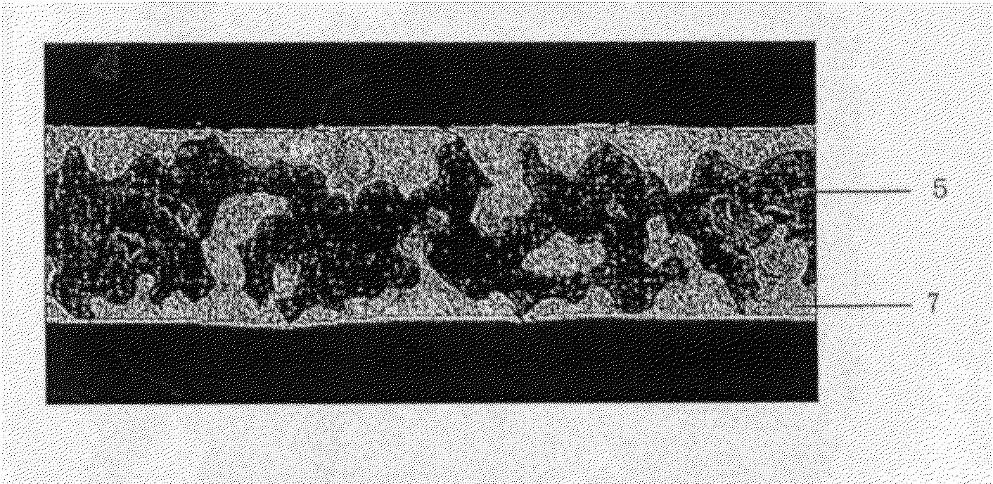
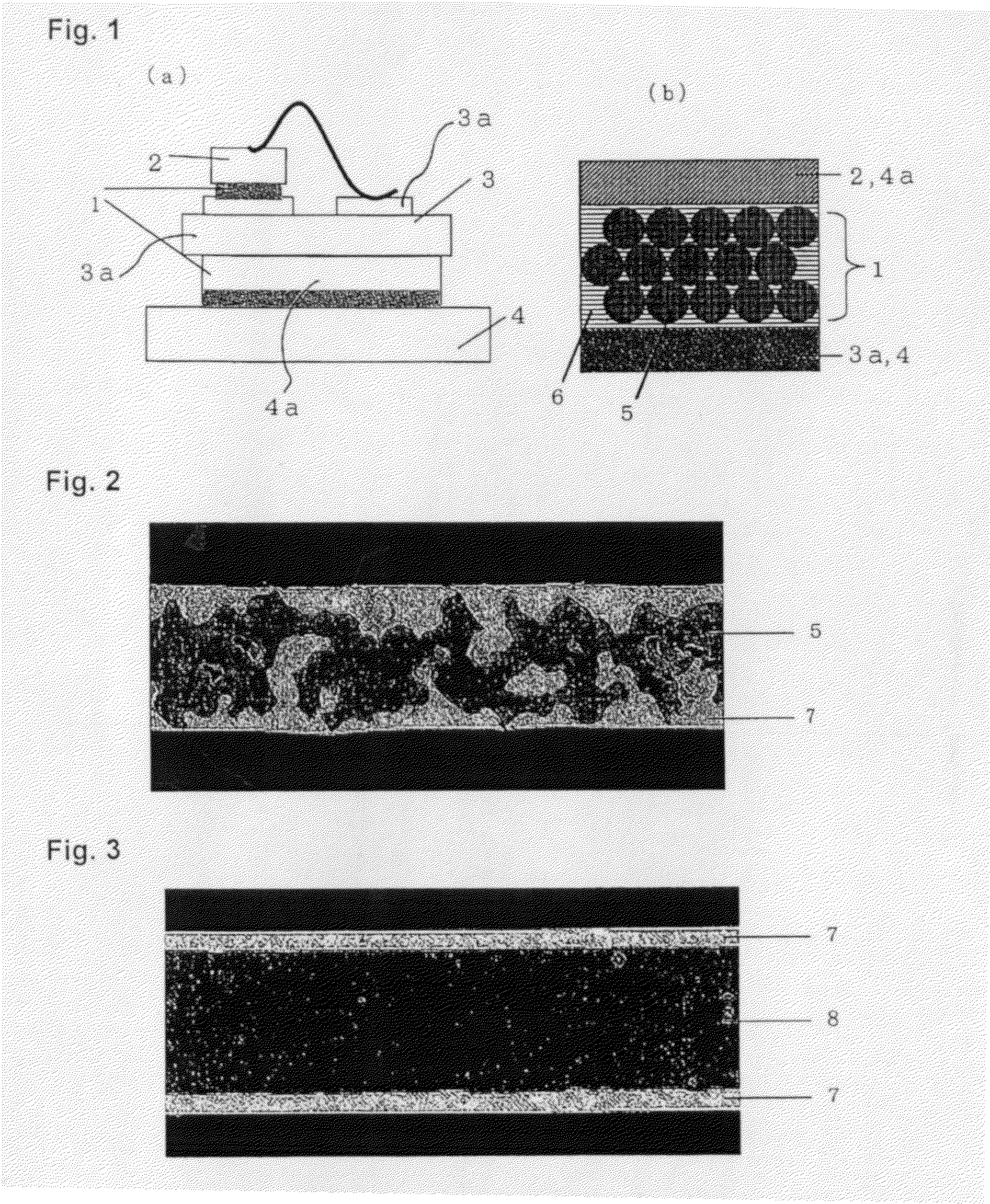
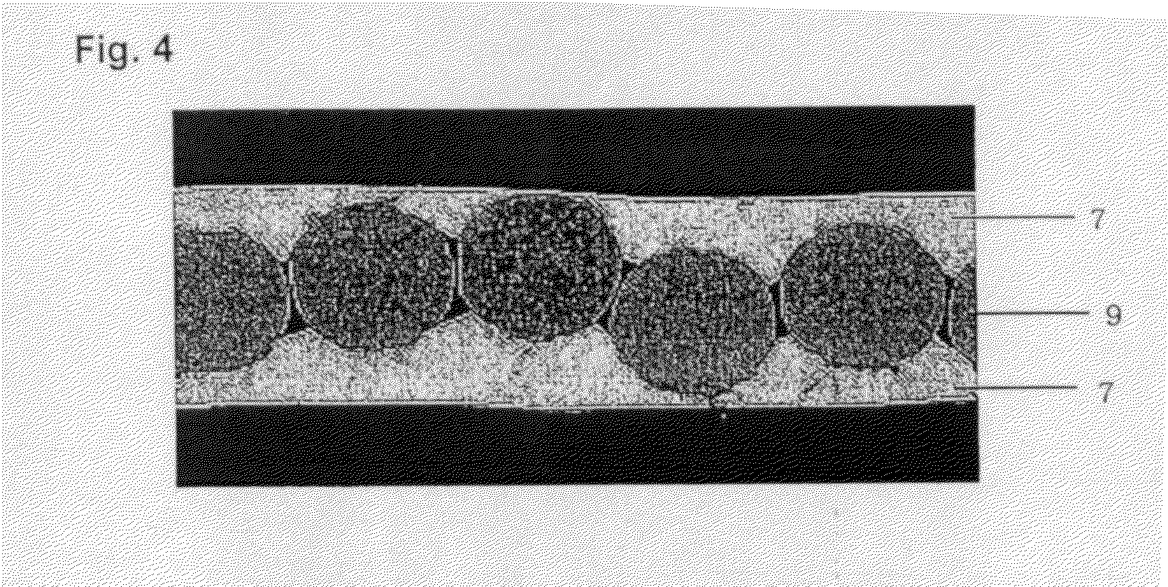
[0066]Phosphorus bronze powder (product name, P-201) manufactured by Fukuda Metal Foil and Powder Company, Ltd. was sintered at 880° C. in a reducing atmosphere to prepare a porous metal body (length of 1 meter, width of 15 mm, thickness of 0.1 mm, porosity of 25%), and it was immersed in various solder baths at 250-260° C. to impregnate its pores with lead-free solder. Flux was not used for impregnation with the molten solder. Instead, an oxide film was removed from the porous metal body by impinging ultrasonic waves in the solder bath, and the formation of voids was prevented. The pore structure of the porous body which was used had continuous pores connected in a mesh-like manner, and the pores opened onto the surface of the plate.

[0067]The thickness of the bonding material, namely, the thickness of the metal body plus the adhered amount of solder was controlled by the speed of removal of the porous metal body from the solder bath. It was adjusted so that the total thickness of t...

example 2

[0076]A bonding material measuring 5 mm×5 mm was punched from the bonding material manufactured in Example 1, it was bonded to a Cu plate or an Ni-plated Cu plate measuring 10 mm×10 mm, an Sn—Cu intermetallic compound was formed to simulate a bonding portion.

[0077]A model IrF-TP high temperature observation apparatus manufactured by Yonekura Seisakusho Co., Ltd. was used for bonding, and heating was carried out with a heating temperature of 350° C. for 15 minutes.

[0078]The amount of intermetallic compounds (IMC) which were formed in the bonding portion which was obtained in this manner was measured. The measurement method used a model JSM-7000F scanning electron microscope manufactured by JEOL Ltd., the region where compounds were present was sensed from the cross section of the bonding portion, the detected area was measured, and made the amount of compounds which were formed (μm2). The results are shown in Table 2.

[0079]In the same manner, the voids percentage of the bonding porti...

example 3

[0086]Using the bonding material manufactured in Example 1 (see Example 1 in Table 2), a silicon chip was bonded to an insulating plate, and a Cu substrate was bonded thereto to form a semiconductor device as shown in FIG. 1. Next, the semiconductor device was mounted on a printed circuit board at a reflow temperature of 240° C.

[0087]The internal bonds of the semiconductor device did not melt at the time of mounting.


PUM

PropertyMeasurementUnit
porosityaaaaaaaaaa
thicknessaaaaaaaaaa
thicknessaaaaaaaaaa

Abstract

A semiconductor device is provided which has internal bonds which do not melt at the time of mounting on a substrate. A bonding material is used for internal bonding of the semiconductor device. The bonding material is obtained by filling the pores of a porous metal body having a mesh-like structure and covering the surface thereof with Sn or an Sn-based solder alloy.

Description

[0001]This is a 371 national stage application of PCT / JP2011 / 067770 filed Aug. 3, 2011, claiming priority to Japanese Patent Application No. 2010-176456 filed Aug. 5, 2010.TECHNICAL FIELD[0002]This invention relates to a solder bonding material used for semiconductor devices and particularly a bonding material for bonding semiconductor elements which require heat dissipation, such as power semiconductors (such as power diodes) or semiconductor chips having fine internal wiring to substrates. This invention also relates to a semiconductor device having a semiconductor element bonded to a substrate with such a bonding material.BACKGROUND ART[0003]Typical examples of semiconductor devices are semiconductor devices in which a semiconductor chip (a silicon chip) is mounted on a frame, i.e., a substrate made of Cu or 42 alloy. Wire bonding using Au wires is carried out between a silicon chip and a frame. Bonding of a frame to a silicon chip sometimes uses an electrically conductive epoxy ...

Claims


Application Information

Patent Timeline
Patent Type & Authority Patents(United States)
IPC IPC(8): C22C1/08B23K35/26H01L23/373H01L23/00C22C13/00B23K35/02C22C9/02B23K35/30H01L23/48H05K3/34
CPCH01L2924/01006C22C9/02H01L2224/83801H01L2924/00013B23K35/262H01L2924/01004H01L24/32H01L2224/48227C22C13/00H01L2224/8309B23K35/025H01L2224/48091B23K35/302H01L24/45H01L2924/01047H01L2224/29101H01L2924/01079H01L2224/29198H01L2924/01322H01L2924/10253H01L2924/01051H01L2924/01078C22C1/08H05K3/3463H01L24/29H01L23/3735H01L24/07H01L24/83H01L2924/0132H01L2224/29H01L2924/01028H01L2224/83065B23K2201/40H01L2924/01327H01L2224/32014H01L2924/01021H01L2924/01082H01L2224/83455H01L2224/2929H01L2224/8384H01L2924/01033H01L2924/01005H01L2224/48472H05K2201/0116B22F2998/00H01L2224/45144H01L2224/32225H01L2224/29299H01L2924/014H01L24/48H01L2224/73265H01L2924/01014H01L2224/83444H01L2924/0105H01L2224/2919H01L2924/01029H01L2924/0665H01L24/73H01L2924/0103H01L2924/15747Y10T428/12479H01L2924/203H01L2224/04042B23K2101/40H01L2924/00014C22C1/0483H01L2924/00H01L2924/00012H01L2224/29099H01L2224/29199H01L2924/0002B23K35/02B23K1/00B23K1/08H01L21/52
Inventor SAKAMOTO, YOSHITSUGUYAMADA, HIROYUKIYAMANAKA, YOSHIEOHNISHI, TSUKASAYOSHIKAWA, SHUNSAKUTADOKORO, KENZO
Owner SENJU METAL IND CO LTD
Why Eureka
Try Eureka