Encapsulation, MEMS and Method of Selective Encapsulation

a technology of selective encapsulation and mems, applied in the direction of microstructural system, instrument, semiconductor/solid-state device details, etc., can solve the problems of complex production method, cost-intensive, and use of three-dimensional structure caps composed of silicon or glass, so as to prevent an areal attachment and increase stability

Inactive Publication Date: 2011-05-26
ROBERT BOSCH GMBH
View PDF8 Cites 16 Cited by
  • Summary
  • Abstract
  • Description
  • Claims
  • Application Information

AI Technical Summary

Benefits of technology

[0020]With regard to the shaping of the cavity, there are various possibilities. Thus, it is conceivable to shape said cavity for example in curved (bent, roundish) fashion. In addition, angular or combined round / angular shapes can be realized. In this case, roundings have an increased stability and prevent an areal attachment and hence adhering of the active structures of the MEMS.

Problems solved by technology

What is common to all the aforementioned methods is that a cost-intensive, three-dimensionally structured cap composed of silicon or glass is used.
What is disadvantageous about the known encapsulation is the complex production method thereof using an alternative film that firstly has to be applied and then has to be removed again.

Method used


Image

  • Encapsulation, MEMS and Method of Selective Encapsulation
  • Encapsulation, MEMS and Method of Selective Encapsulation
  • Encapsulation, MEMS and Method of Selective Encapsulation

Examples


Embodiment Construction

[0031]In the figures, identical components and components having the same function are identified by the same reference signs.

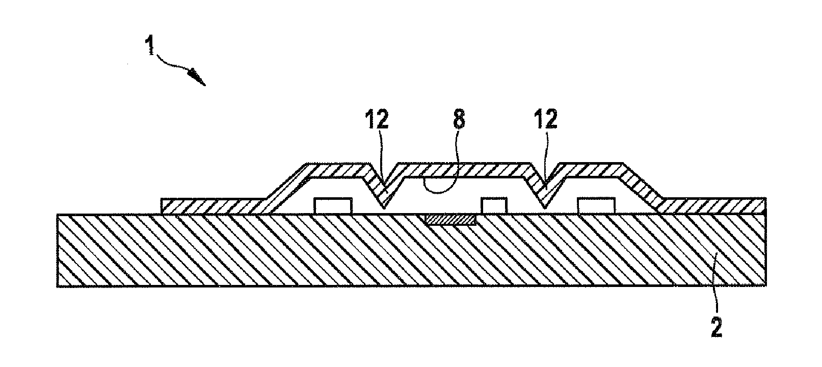
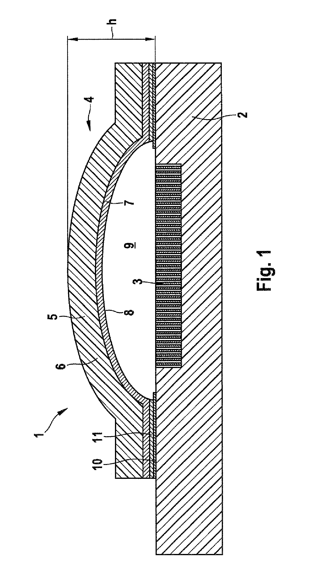
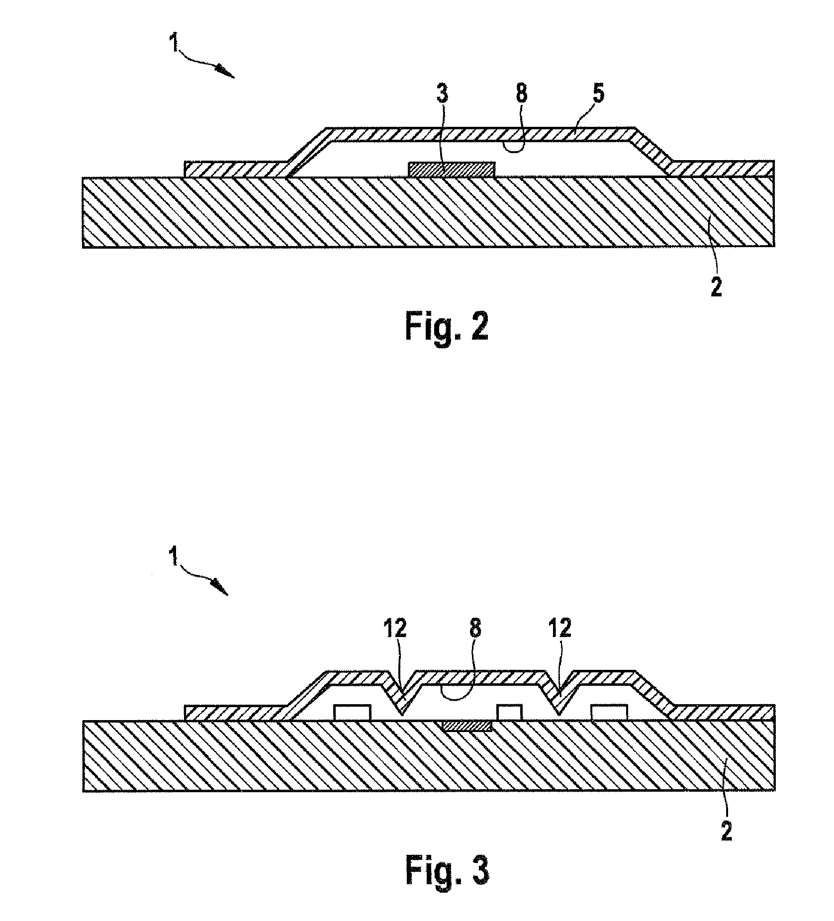
[0032]FIG. 1 shows an MEMS 1 (Microelectromechanical System). The MEMS 1 comprises a semiconductor substrate 2 with a sensitive, mechanical, component structure formed thereon, said component structure being formed from a semiconductor material. The component structure 3 is protected against mechanical and other environmental influences, such as temperature and moisture and also gas, by an encapsulation 4. The height h of the encapsulation 4 (measured perpendicularly to the areal extent of the semiconductor substrate 2) is approximately 200 μm in the exemplary embodiment. The encapsulation 4 is formed with the aid of a film 5 embodied as a multilayer film. Said film comprises a polymer layer 6, here composed of LCP, and also an outer metal layer 7, here composed of ductile copper, which faces the semiconductor substrate 2. The film 5 is distinguished by a thr...


PUM


Abstract

The invention relates to an encapsulation (4) of a sensitive component structure (3) on a semiconductor substrate (2) with a film (5) covering the component structure (3). According to the invention, it is provided that a cavity (8) for the component structure (3) is provided in the film (5). The invention also relates to a MEMS (1) and to a method for encapsulating a sensitive component structure (3).

Description

PRIOR ART[0001]The invention relates to an encapsulation in accordance with the preamble of claim 1, a microelectromechanical system (MEMS), in accordance with claim 18, and a method for encapsulating a sensitive component structure on a semiconductor substrate in accordance with claim 19.[0002]Sensitive, mainly mechanical, component structures of MEMS have to be encapsulated for protection against damage. Inertial sensors, such as acceleration sensors or rate-of-rotation sensors, are currently covered with KOH-etched silicon caps, the caps being connected with the aid of a seal glass connection on the semiconductor substrate having the sensitive component structure. A further established method for encapsulating sensitive component structures on semiconductor substrates is the anodic bonding of three-dimensionally structured glass wafers. In addition, structured silicon wafers as encapsulation are fixed to semiconductor substrates by various bonding methods. What is common to all t...

Claims


Application Information

Patent Timeline
Patent Type & Authority Applications(United States)
IPC IPC(8): H01L29/84H01L21/02
CPCB81C1/00269B81C2203/0109B81C2203/019G01P1/023H01L23/3135H01L2924/0002H01L23/315H03H9/1057H01L2924/00
Inventor ROTHACHER, PETER
Owner ROBERT BOSCH GMBH
Why Eureka
Try Eureka