Semiconductor device and method for manufacturing the same

a semiconductor and on-current technology, applied in semiconductor devices, instruments, electrical equipment, etc., can solve the problems of insufficient ratio of on-current to off-current, change in transistor characteristics such as threshold values, etc., and achieve excellent productivity and higher reliability.

Active Publication Date: 2011-06-02
SEMICON ENERGY LAB CO LTD
View PDF99 Cites 106 Cited by
  • Summary
  • Abstract
  • Description
  • Claims
  • Application Information

AI Technical Summary

Benefits of technology

[0047]Furthermore, a semiconductor device having excellent productivity can be provided.
[0048]Furthermore, a semiconductor device having higher reliability can be provided.

Problems solved by technology

However, in a transistor including an oxide semiconductor which easily responds to an increase in size of a manufacturing substrate and has high electric field-effect mobility, when the oxide semiconductor is connected to a copper wiring having low wiring resistance, a problem is caused that the ratio of on current to off current is not sufficient and remains in a figure of approximately 103.
In addition, there is another problem in that an impurity enters the inside of the transistor from the outside after long-term use, resulting in change in transistor characteristics such as a threshold value.

Method used


Image

  • Semiconductor device and method for manufacturing the same
  • Semiconductor device and method for manufacturing the same
  • Semiconductor device and method for manufacturing the same

Examples


embodiment 1

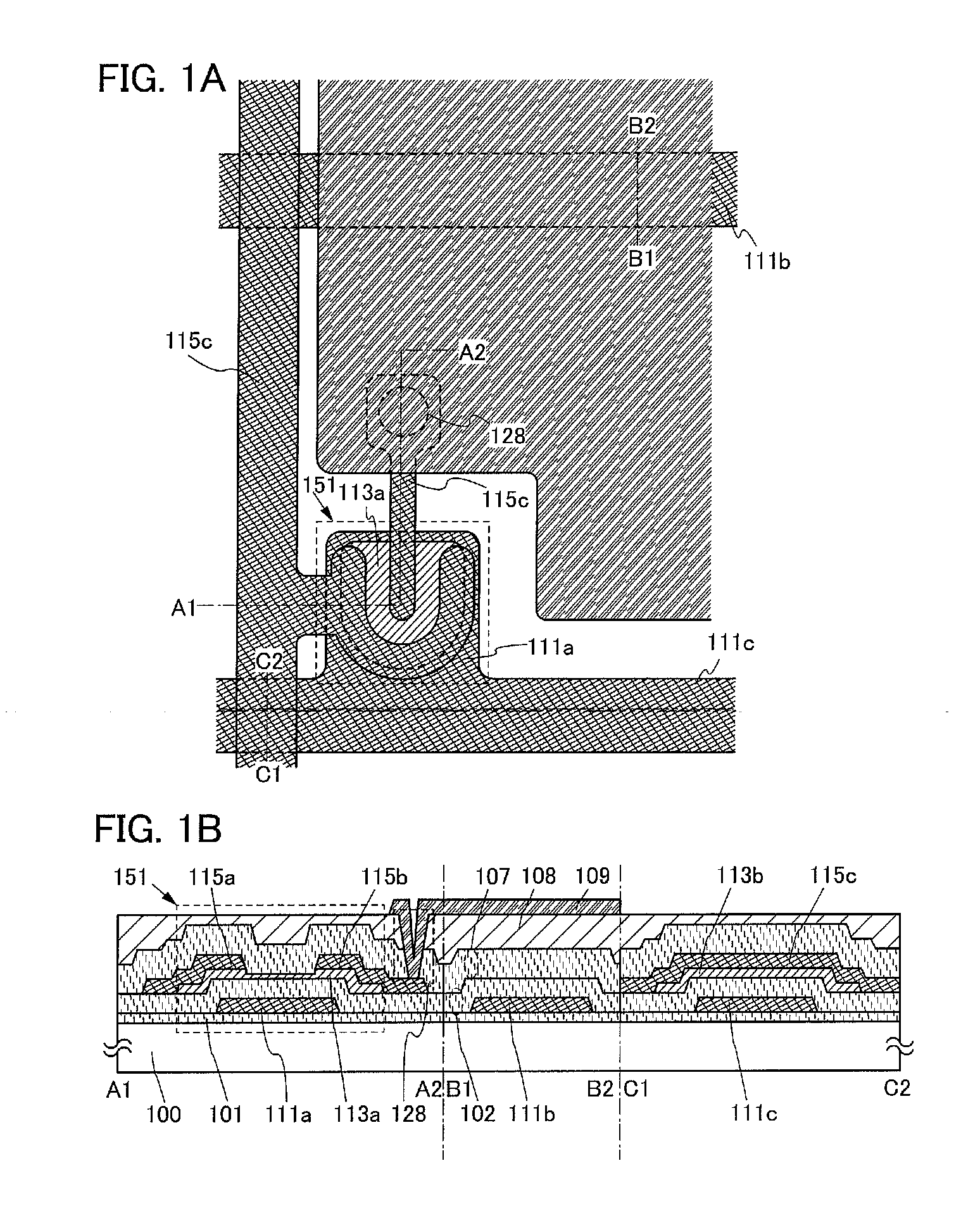
[0090]In this embodiment, one embodiment of a substrate provided with a circuit of a display device will be described as one embodiment of a semiconductor device, with reference to FIGS. 1A and 1B.

[0091]A structure of a pixel provided in the display device is illustrated in FIGS. 1A and 1B. FIG. 1A is a top view illustrating a plan structure of the pixel, and FIG. 1B is a cross-sectional view illustrating a stacked structure in the pixel. Note that chain lines A1-A2, B1-B2, and C1-C2 in FIG. 1A correspond to cross sections A1-A2, B1-B2, and C1-C2 in FIG. 1B, respectively.

[0092]In the cross section A1-A2, a stacked structure in a transistor 151 used in the pixel portion is illustrated. The transistor 151 is one embodiment of a transistor having a bottom gate structure.

[0093]In the cross section B1-B2, a stacked structure in a capacitor formed in the pixel portion is illustrated.

[0094]Further, in the cross section C1-C2, a stacked structure in a wiring intersection portion of a gate w...

embodiment 2

[0193]In this embodiment, a manufacturing process of the semiconductor device described in Embodiment 1 will be described with reference to FIGS. 13A to 13E. Note that cross sections A1-A2, B1-B2, and C1-C2 in FIGS. 13A to 13E are cross-sectional views taken along chain lines A1-A2, B1-B2, and C1-C2 in FIG. 1A, respectively.

[0194]First, the base film 101 including silicon nitride is formed to a thickness greater than or equal to 50 nm and less than or equal to 300 nm, preferably greater than or equal to 100 nm and less than or equal to 200 nm over the substrate 100. As the substrate 100, other than a glass substrate or a ceramic substrate, a plastic substrate or the like with heat resistance which can withstand a process temperature in this manufacturing process can be used. In the case where the substrate does not need a light-transmitting property, a metal substrate such as a stainless steel alloy substrate, provided with an insulating film on its surface may be used. As the glass...

embodiment 3

[0268]In this embodiment, one embodiment of a substrate provided with a circuit of a display device which has a structure different from that of Embodiment 1 will be described with reference to FIGS. 15A and 15B.

[0269]A structure of a pixel in the display device is illustrated in FIGS. 15A and 15B. FIG. 15A is a top view illustrating a plan structure of the pixel, and FIG. 15B is a cross-sectional view illustrating a stacked structure in the pixel. Note that chain lines A1-A2, B1-B2, and C1-C2 in FIG. 15A correspond to cross sections A1-A2, B1-B2, and C1-C2 in FIG. 15B, respectively.

[0270]In the cross section A1-A2, a stacked structures in a transistor 152 used in the pixel portion is illustrated. The transistor 152 is one embodiment of a transistor having a bottom gate structure.

[0271]In the cross section B1-B2, a stacked structure in a capacitor formed in the pixel portion is illustrated.

[0272]Further, in the cross section C1-C2, a stacked structure in an intersection portion of a...


PUM


Abstract

Disclosed is a semiconductor device comprising a thin film transistor and wirings connected to the thin film transistor, in which the thin film transistor has a channel formation region in an oxide semiconductor layer, and a copper metal is used for at least one of a gate electrode, a source electrode, a drain electrode, a gate wiring, a source wiring, and a drain wiring. The extremely low off current of the transistor with the oxide semiconductor layer contributes to reduction in power consumption of the semiconductor device. Additionally, the use of the copper metal allows the combination of the semiconductor device with a display element to provide a display device with high display quality and negligible defects, which results from the low electrical resistance of the wirings and electrodes formed with the copper metal.

Description

TECHNICAL FIELD[0001]The present invention relates to a semiconductor device including a semiconductor element and a manufacturing method thereof.[0002]Note that a semiconductor device in this specification indicates all the devices that can operate by using semiconductor characteristics, and semiconductor elements such as transistors; and electro-optical devices, semiconductor circuits, and electronic appliances which include the semiconductor element are all included in the category of the semiconductor devices.BACKGROUND ART[0003]In recent years, a technique by which transistors are manufactured using an oxide semiconductor as a semiconductor material and the transistors are applied to semiconductor circuits, ICs, electro-optical devices, electronic appliances and the like has attracted attention.[0004]For example, Patent Document 1 and Patent Document 2 disclose a technique with which a thin film transistor (also referred to as a TFT) is manufactured using a semiconductor thin f...

Claims


Application Information

Patent Timeline
Patent Type & Authority Applications(United States)
IPC IPC(8): H01L29/12
CPCG02F1/1368H01L27/1225H01L27/3262H01L29/7869H01L27/124H01L33/0041H01L2924/0002H01L2924/00H10K59/1213H01L29/4908H01L27/1214H01L29/45H01L29/78606
Inventor YAMAZAKI, SHUNPEIHOSOBA, MIYUKIHIRAISHI, SUZUNOSUKE
Owner SEMICON ENERGY LAB CO LTD
Why Eureka
Try Eureka