Dielectric resonator antenna embedded in multilayer substrate

a technology of dielectric resonator and multi-layer substrate, which is applied in the direction of resonators, antenna details, antennas, etc., can solve the problems of poor product reliability, increased antenna characteristics due to fabrication errors, and difficult fabrication of antennas, so as to facilitate fabrication and reduce the effect of fabrication errors

Inactive Publication Date: 2011-06-09
SAMSUNG ELECTRO MECHANICS CO LTD
View PDF16 Cites 55 Cited by
  • Summary
  • Abstract
  • Description
  • Claims
  • Application Information

AI Technical Summary

Benefits of technology

[0016]Accordingly, the present invention has been made keeping in mind the problems encountered in the related art and the present invention is intended to provide a dielectric resonator antenna embe

Problems solved by technology

However, if the substrate is burned during the fabrication of the LTCC, it may shrink by about 15% in the directions of x and y which are the planar directions of the substrate, undesirably causing a fabrication error resulting in poor reliability of products.
In multilayer structures such as LTCC and LCP, a patch antenna having planar characteristics is mainly used, but is problematic because of a narrow bandwidth of about 5%.
However, in the case of using multi-resonance, there may occur a difference in radiation patte

Method used


Image

  • Dielectric resonator antenna embedded in multilayer substrate
  • Dielectric resonator antenna embedded in multilayer substrate
  • Dielectric resonator antenna embedded in multilayer substrate

Examples


first embodiment

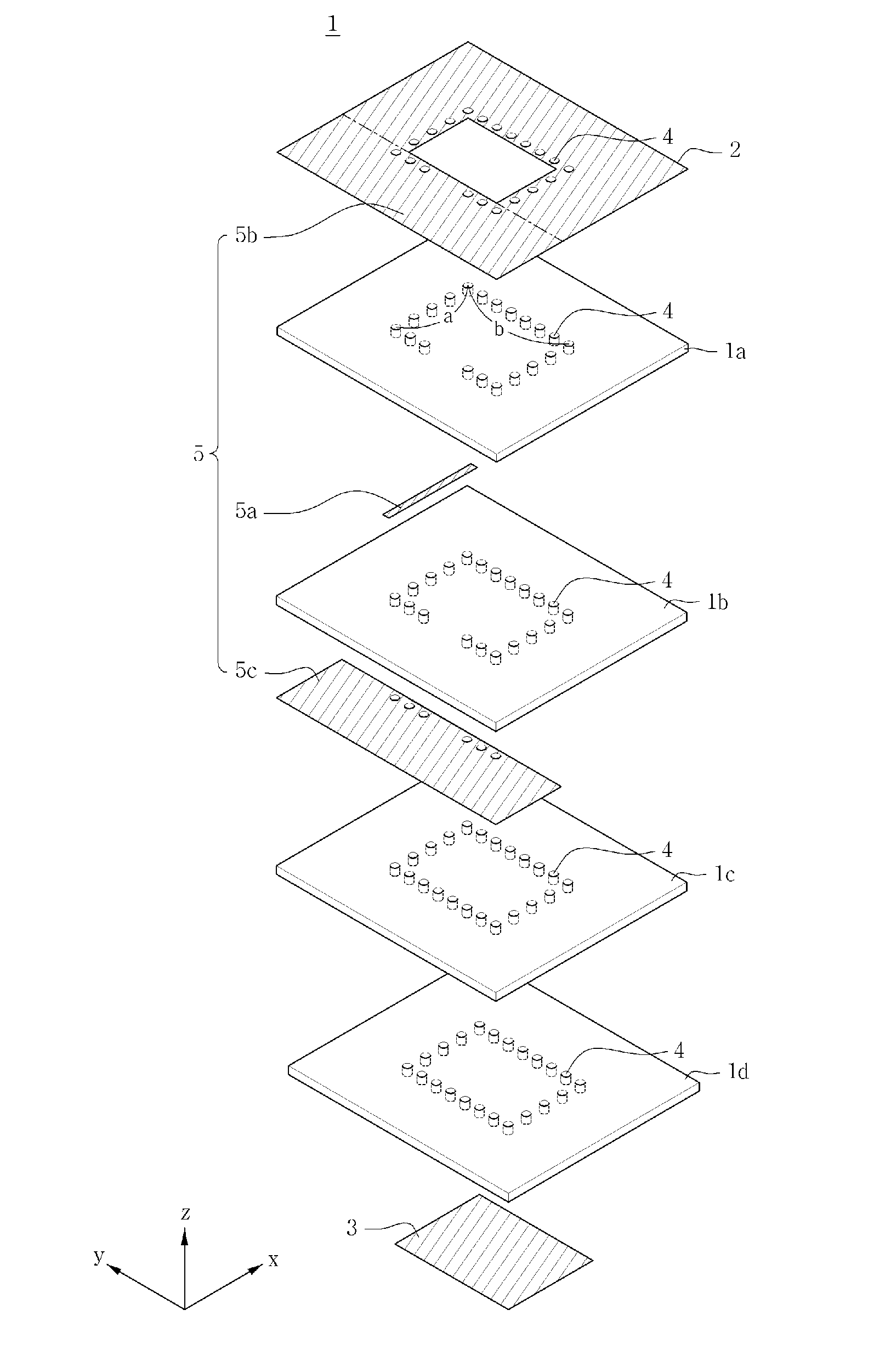
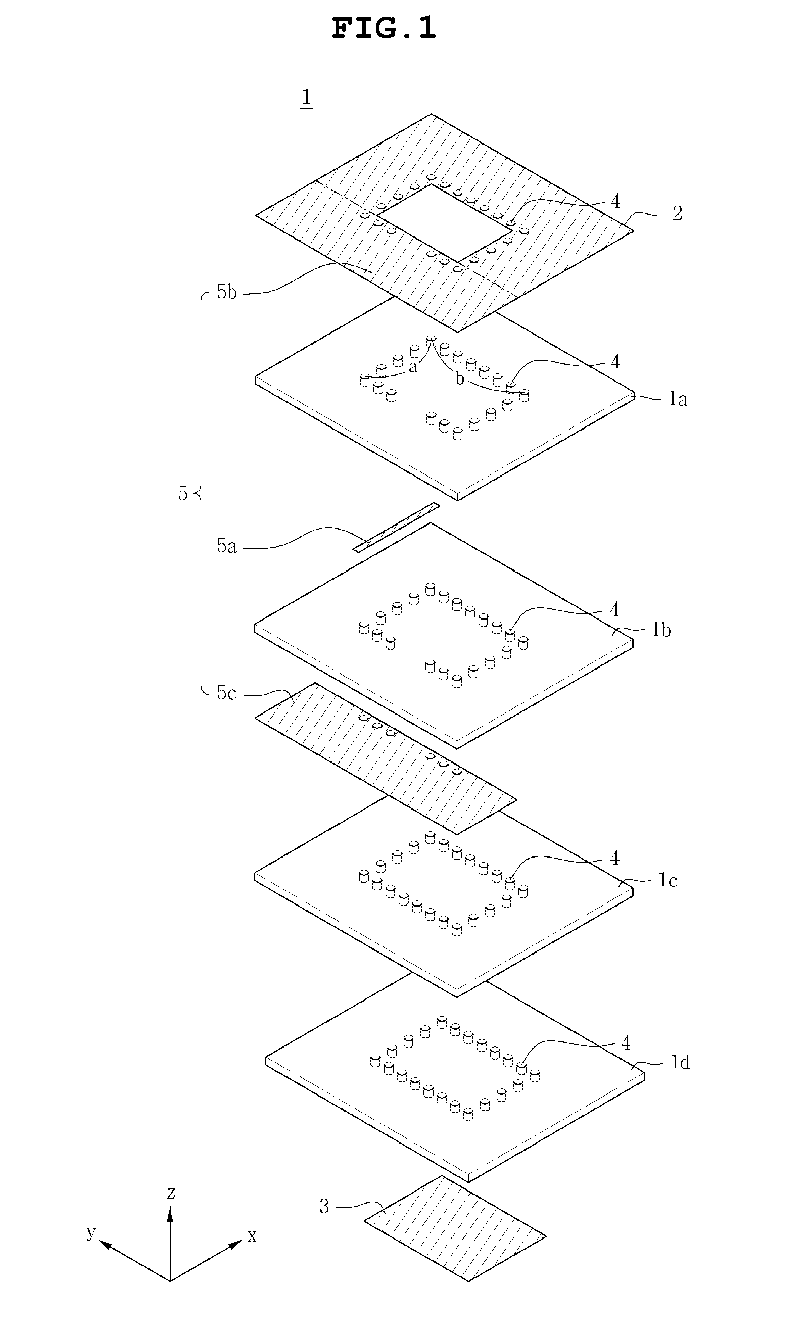
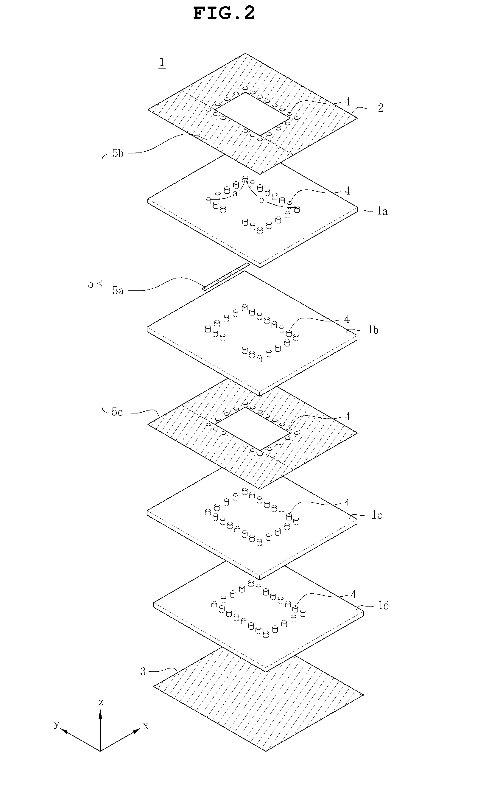
[0057]FIGS. 1 and 2 are exploded perspective views showing examples of a dielectric resonator antenna embedded in a multilayer substrate according to the present invention, FIG. 3 is a top plan view of FIG. 1, and FIGS. 4 and 5 are respectively cross-sectional views of FIG. 1 and FIG. 2 taken along the line A-A′ of FIG. 3.

[0058]With reference to FIGS. 1 and 2, the dielectric resonator antenna embedded in the multilayer substrate according to the first embodiment of the present invention includes a multilayer substrate 1, a first conductor plate 2 having an opening in the center thereof and formed on the top of the uppermost insulating layer 1a of the multilayer substrate 1, a second conductor plate 3 located on the bottom of the lowermost insulating layer 1d of the multilayer substrate 1, a plurality of metal via holes 4 passing through from the uppermost insulating layer 1a to the lowermost insulating layer 1d, and a feeder 5 including a feed line 5a and at least one ground plate 5...

second embodiment

[0109]FIG. 9 is a top plan view showing a dielectric resonator antenna embedded in a multilayer substrate 61 according to the present invention, in which the dielectric resonator has a cylinder shape.

[0110]In this case, the dielectric resonator includes a multilayer substrate 61, a first conductor plate 62, a second conductor plate 63, a plurality of metal via holes 64 for electrically connecting layers of the multilayer substrate 61, and a feed line 65a, as in the dielectric resonator antenna of FIGS. 1 to 5.

[0111]This dielectric resonator antenna has the same constituents and exhibits the same functions as in the dielectric resonator antenna embedded in the multilayer substrate 1 according to the first embodiment as shown in FIGS. 1 to 5, with the exception of the shape of the opening of the first conductor plate 62, and the detailed description thereof is thus omitted.

[0112]The dielectric resonator antenna embedded in the multilayer substrate 61 according to the second embodiment...


PUM


Abstract

Disclosed is a dielectric resonator antenna embedded in a multilayer substrate, which includes a multilayer substrate, a first conductor plate having an opening, a second conductor plate formed on the bottom of a lowermost insulating layer resulting from stacking at least two insulating layers downward from the first conductor plate, a plurality of metal via holes passing through around the opening at a predetermined interval, and a feeder for transmitting a frequency signal to the dielectric resonator embedded by the metal boundaries defined by the first conductor plate, the second conductor plate and the plurality of metal via holes, thus exhibiting low sensitivity to fabrication error and the external environment.

Description

CROSS REFERENCE TO RELATED APPLICATION[0001]This application claims the benefit of Korean Patent Application No. 10-2009-0121323, filed Dec. 8, 2009, entitled “Dielectric resonator antenna embedded in multilayer substrate”, which is hereby incorporated by reference in its entirety into this application.BACKGROUND OF THE INVENTION[0002]1. Technical Field[0003]The present invention relates to a dielectric resonator antenna embedded in a multilayer substrate.[0004]2. Description of the Related Art[0005]Conventional transmission and receiving systems are mostly fabricated by assembling respective components. However, research into system-on-package products in which a transmission and receiving system of the millimeter wave band is fabricated into a single package is being conducted these days, and part of the products is commercially available.[0006]Technology for single package products has been developed together with multilayer substrate fabrication techniques for stacking dielectri...

Claims


Application Information

Patent Timeline
IPC IPC(8): H01Q9/04
CPCH01Q13/00H01Q9/0485H01P7/10H01Q1/38H01Q13/08
Inventor LEE, JUNG AUNKIM, MOONILLEE, KOOK JOOPARK, CHUL GYUN
Owner SAMSUNG ELECTRO MECHANICS CO LTD
Why Eureka
Try Eureka