
Connection structure for chip-on-glass driver IC and connection method therefor

a technology of chip-on-glass and connection structure, which is applied in the direction of semiconductor devices, semiconductor/solid-state device details, basic electric elements, etc., can solve the problem of easy generation of short-circuit problems, and achieve the effects of reducing the risk of forming, enhancing connection strength, and increasing contact area

Inactive Publication Date: 2011-06-09
HANNSTAR DISPLAY CORPORATION
View PDF22 Cites 1 Cited by
  • Summary
  • Abstract
  • Description
  • Claims
  • Application Information

AI Technical Summary

Benefits of technology

[0007]A primary object of the present invention is to provide a connection structure for a chip-on-glass (COG) driver IC, wherein a surface of a driver IC is provided with polymeric bumps to increase the contact area between the driver IC and an adhesive film and to enhance the connection strength of the adhesive film for holding the driver IC, so as to overcome the thermal stress generated during the process of thermal compression bonding and to reduce the risk of forming vacuum holes generated between conductive bumps and pads. As a result, the connection reliability between the conductive bumps and the pads can be enhanced, and the packaging yield of the driver IC can be improved.
[0008]A secondary object of the present invention is to provide a connection structure for a COG driver IC and a connection method therefor, wherein photosensitive polymer is used to form a polymer layer which is processed by processes of exposure and development to form a plurality of polymeric bumps, so as to simplify the process of the polymeric bumps and increase the height uniformity of the polymeric bumps.

Problems solved by technology

However, the disadvantages of the driver IC 13 are described, as follows: when the pitch of the gold bumps 131 is reduced and the distribution density thereof is increased, a short-circuit problem may be easily generated due to the conductive particles 121 disposed between each two of the adjacent gold bumps 131 which may unexpectedly connect the adjacent gold bumps 131 with each other.

Method used


Image

  • Connection structure for chip-on-glass driver IC and connection method therefor
  • Connection structure for chip-on-glass driver IC and connection method therefor
  • Connection structure for chip-on-glass driver IC and connection method therefor

Examples


Embodiment Construction

[0036]The present invention discloses a connection structure for a chip-on-glass (COG) driver IC and a connection method therefor, both of which can be applied to technologies fields of various image display devices or image capturing devices, wherein the image display devices can be selected from liquid crystal display (LCD), plasma display panel (PDP), digital light processing (DLP), electro-phoretic display (EPD, i.e. electronic paper display) or other display devices, while the image capturing devices can be selected from camera lens module, video camera lens module or other image sensors, but not limited thereto.

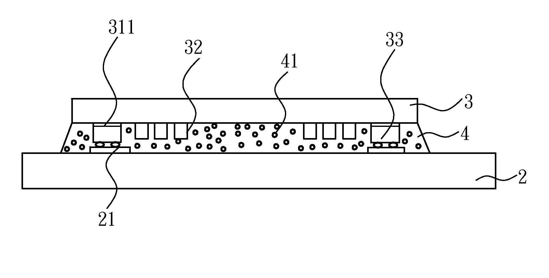
[0037]Referring now to FIGS. 4A and 4B, a connection structure for a chip-on-glass (COG) driver IC according to a first embodiment of the present invention is illustrated. As shown, the connection structure comprises a glass substrate 2, a driver IC 3 and an adhesive film 4, wherein the glass substrate 2 is preferably selected from a glass plate having a transparent con...


PUM


Abstract

A connection structure for a chip-on-glass (COG) driver IC and a connection method therefor are provided. The connection structure includes a driver IC having a surface provided with a plurality of polymeric bumps and a plurality of conductive bumps, and the height of the polymeric bumps in relation to the surface is smaller than that of the conductive bumps. When the driver IC is bonded to a glass substrate via an adhesive film by thermal compression bonding, the polymeric bumps are embedded into the adhesive film, and a gap is defined between the polymeric bumps and the glass substrate. Thus, the polymeric bumps can increase the contact area between the driver IC and the adhesive film, and enhance the connection reliability between the conductive bumps and pads of the glass substrate.

Description

FIELD OF THE INVENTION[0001]The present invention relates to a connection structure for a chip-on-glass (COG) driver IC and a connection method therefor, and more particularly to a connection structure for a COG driver IC having polymeric bumps to increase the connection reliability thereof when connecting to a glass substrate via an adhesive film and a connection method for the COG driver IC.BACKGROUND OF THE INVENTION[0002]Presently, various audio video electronic products are now in widespread use, so as to further promote the rapid development of various image display technologies, wherein common image display technologies includes liquid crystal display (LCD), plasma display panel (PDP), digital light processing (DLP) and etc. The foregoing image display technologies are generally applied to various electronic products, such as computer monitors, televisions, mobile phones, digital cameras, digital video cameras, MP3 players, game consoles, other 3C products and etc. The develo...

Claims


Application Information

Patent Timeline
Patent Type & Authority Applications(United States)
IPC IPC(8): H05K7/12
CPCH01L2224/13099H01L2924/07802H01L2924/01078H01L2924/01079H01L2924/14H01L2224/13076H01L2224/26125H01L23/16H01L24/13H01L24/16H01L24/29H01L24/32H01L24/73H01L24/81H01L24/83H01L24/92H01L2224/10126H01L2224/13007H01L2224/13019H01L2224/13144H01L2224/1319H01L2224/2919H01L2224/73204H01L2224/81191H01L2224/81801H01L2224/83192H01L2224/8385H01L2224/83851H01L2224/9211H01L2924/01049H01L2224/0401H01L2224/02166H01L2224/13565H01L2224/13011H01L2924/10253H01L2224/293H01L2224/2929H01L2924/01006H01L2924/01033H01L2924/00013H01L2924/00014H01L2224/81H01L2224/83H01L2224/13599H01L2224/05599H01L2224/05099H01L2224/29099H01L2224/29599H01L2924/00H01L2924/351H01L2924/15788
Inventor SUN, WEI-HAOTANG, PAO-YUN
Owner HANNSTAR DISPLAY CORPORATION
Learn More