
Semiconductor device

a technology of semiconductor devices and switching transistors, applied in semiconductor devices, semiconductor/solid-state device details, pulse techniques, etc., can solve the problems of difficult to make the standby power of a cmos circuit substantially zero in the technique, and the leakage current of the switching transistor itself is not practicable, and the effect of reducing the standby power of the cmos circui

Inactive Publication Date: 2011-06-16
SEMICON ENERGY LAB CO LTD
View PDF99 Cites 43 Cited by
  • Summary
  • Abstract
  • Description
  • Claims
  • Application Information

AI Technical Summary

Benefits of technology

[0005]Standby power depends on the leakage current of the switching transistor in the technique disclosed in Patent Document 1. That is, standby power can be sufficiently reduced by sufficiently reducing the leakage current of the switching transistor.
[0010]In the disclosed invention, a semiconductor device (for example, a transistor) is formed using a highly purified oxide semiconductor. The leakage current of the transistor formed using a highly purified oxide semiconductor is extremely small, so that on / off ratio can be sufficiently increased. In other words, the leakage current of the transistor can be kept at extremely low level even when current drive capability of the transistor is sufficiently secured.
[0024]In the disclosed invention, a highly purified oxide semiconductor is used for a semiconductor device. “Highly purified” is a concept including at least one of the following: to remove hydrogen in an oxide semiconductor from the oxide semiconductor layer as much as possible; or to supply oxygen, which is in short supply in an oxide semiconductor, into the oxide semiconductor so that defect level in energy gap due to oxygen deficiency in the oxide semiconductor is reduced.
[0026]In addition, at least part of a semiconductor device is formed including the highly purified oxide semiconductor as described above, so that a semiconductor device whose standby power is sufficiently reduced can be realized. It can be said that effect of the suppression of standby power increases as a circuit becomes complicated.

Problems solved by technology

In view of the above problems, a method for suppressing the leakage current of a switching transistor itself by making the channel width of the switching transistor smaller than that of a transistor included in an integrated circuit is not practical.
Thus, it is difficult to make standby power of a CMOS circuit substantially zero in the technique disclosed in Patent Document 1.
Thus, there is a problem in that a slight amount of standby power of each circuit included in an integrated circuit accumulates to be a large amount of standby power in an integrated circuit including a group of a number of circuits or the like.

Method used


Image

  • Semiconductor device
  • Semiconductor device
  • Semiconductor device

Examples


embodiment 1

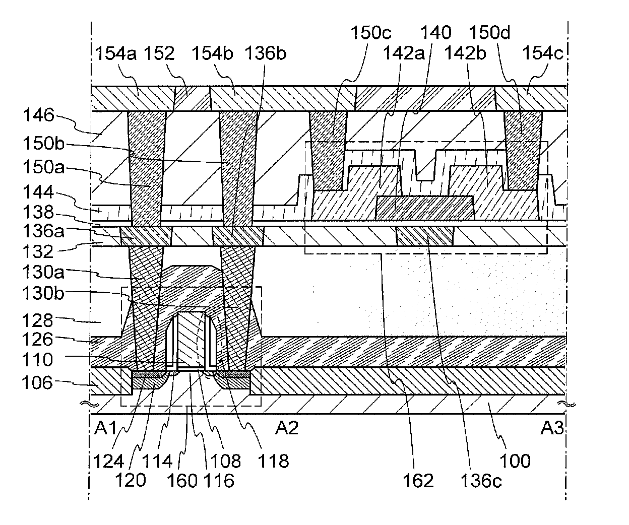
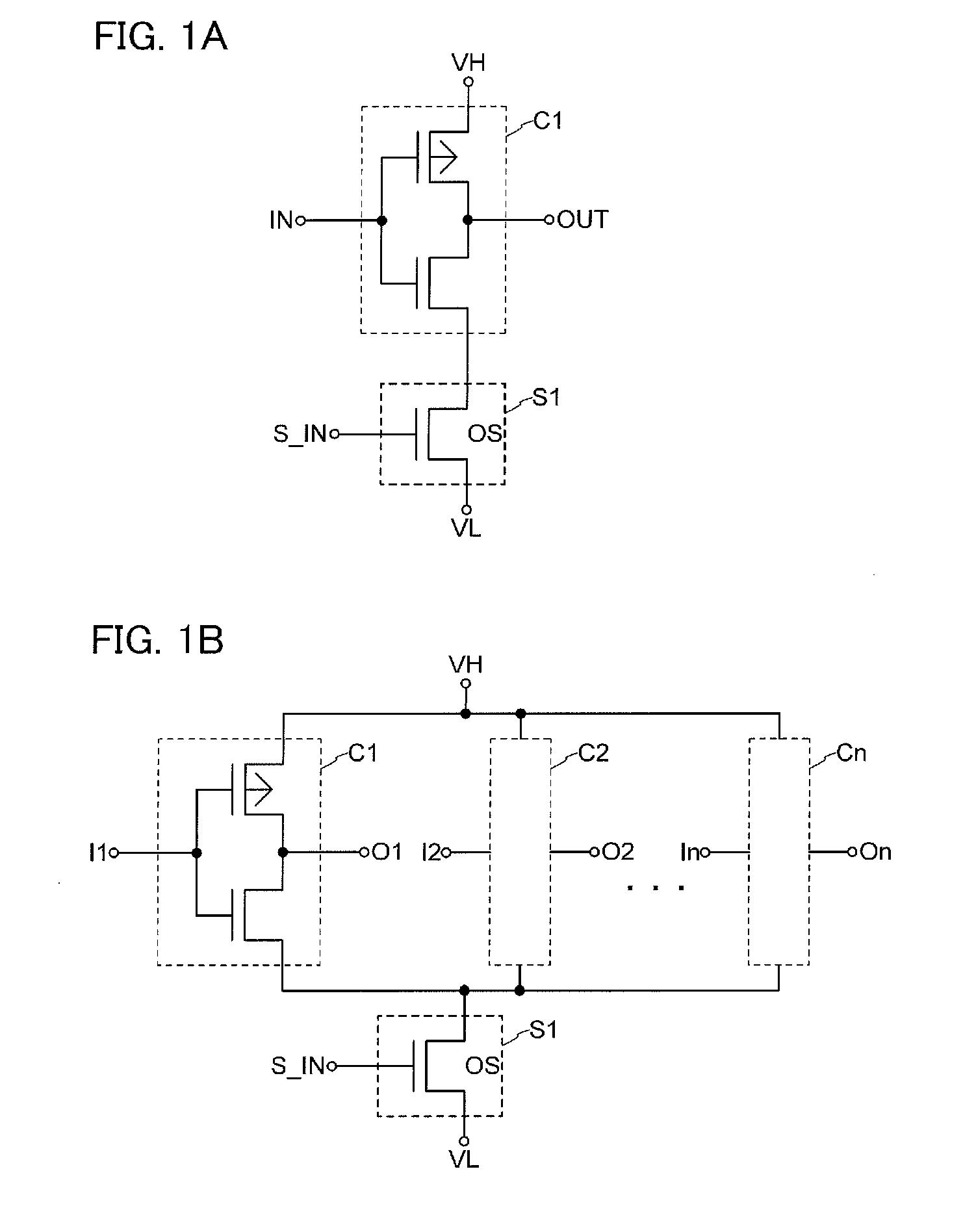
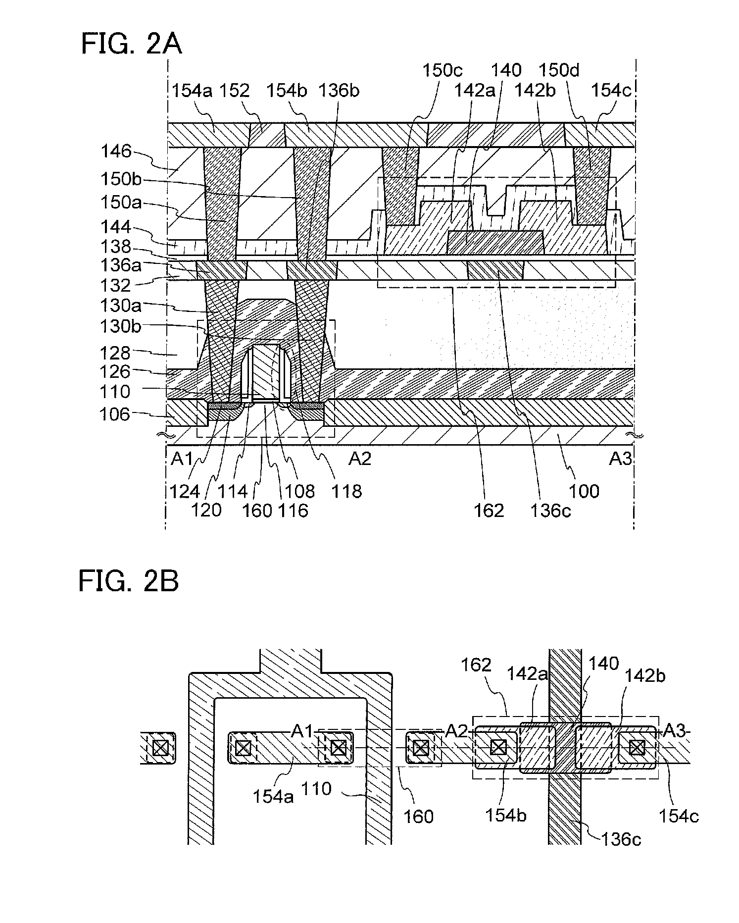
[0042]In this embodiment, a structure and a manufacturing method of a semiconductor device according to one embodiment of the present invention disclosed will be described with reference to FIGS. 1A and 1B, FIGS. 2A and 2B, FIGS. 3A to 3H, FIGS. 4A to 4G and FIGS. 5A to 5D. Note that in a circuit diagram, “OS” is written beside a transistor in order to indicate that the transistor includes an oxide semiconductor.

[0043]FIGS. 1A and 1B show an example of a circuit configuration of a semiconductor device. FIG. 1A is an example of a semiconductor device using a CMOS inverter circuit which is the simplest CMOS circuit. FIG. 1B is an example of a semiconductor device having a plurality of CMOS inverter circuits.

[0044]A semiconductor device shown in FIG. 1A includes a power supply terminal VH, a power supply terminal VL, a switching transistor S1 using an oxide semiconductor material and a CMOS inverter circuit C1. The switching transistor S1 is typically an n-channel transistor using an o...

embodiment 2

[0136]In this embodiment, a semiconductor device having a different configuration from that of the semiconductor device shown in the above embodiment is described with reference to FIGS. 6A and 6B and FIG. 7.

[0137]FIGS. 6A and 6B show an example of a circuit configuration of a semiconductor device according to this embodiment. FIG. 6A is an example of a semiconductor device using a CMOS inverter circuit which is the simplest CMOS circuit. FIG. 6B is an example of a semiconductor device having a plurality of CMOS inverter circuits.

[0138]A difference between the semiconductor devices shown in FIGS. 6A and 6B and the semiconductor devices shown in FIGS. 1A and 1B is whether the switching transistor S1 using an oxide semiconductor has a back gate or not. In the semiconductor device shown in FIGS. 6A and 6B, the switching transistor S1 has a back gate, so that the threshold voltage of the switching transistor S1 can be controlled by controlling a potential of the back gate. Consequently,...

embodiment 3

[0144]In this embodiment, an integrated semiconductor device which is another embodiment of the disclosed invention is described with reference to FIG. 8.

[0145]An integrated semiconductor device 170 which is a modification example of the semiconductor device shown in the foregoing embodiment (for example, Embodiment 1) is shown in FIG. 8. Specific examples of the integrated semiconductor device 170 are a CPU, an MPU and the like.

[0146]The semiconductor device 170 includes a plurality of circuit blocks such as circuit blocks 171 to 174 and the like. In addition, the circuit blocks are electrically connected to each other through an element using an oxide semiconductor at least in a part thereof such as a switching element 181, a switching element 182 and the like.

[0147]For the circuit blocks 171 to 174, an integrated circuit including the CMOS inverter circuits C1 to Cn and the like can be used, for example. Alternatively, a memory circuit or the like typified by DRAM may also be app...


PUM


Abstract

One object is to provide a new semiconductor device whose standby power is sufficiently reduced. The semiconductor device includes a first power supply terminal, a second power supply terminal, a switching transistor using an oxide semiconductor material and an integrated circuit. The first power supply terminal is electrically connected to one of a source terminal and a drain terminal of the switching transistor. The other of the source terminal and the drain terminal of the switching transistor is electrically connected to one terminal of the integrated circuit. The other terminal of the integrated circuit is electrically connected to the second power supply terminal.

Description

TECHNICAL FIELD[0001]The technical field of the disclosed invention relates to a semiconductor device using an oxide semiconductor. The semiconductor device in this specification indicates all the devices that operate by utilizing semiconductor characteristics. For example, a semiconductor device widely includes the following elements: a semiconductor element (including a so-called power device) such as a transistor, a diode and a thyristor, an integrated circuit such as an image sensor, a memory and a converter, an integrated circuit including the above elements and a display device and the like typified by a liquid crystal display device.BACKGROUND ART[0002]A CMOS circuit is a necessary component for a semiconductor integrated circuit because a CMOS circuit has low power consumption and can operate at high speed and can be highly integrated. On the other hand, in recent years, in accordance with miniaturization of a MOS transistor, an increase of power consumption at the time when...

Claims


Application Information

Patent Timeline
IPC IPC(8): H01L27/088
CPCH01L27/0688H01L27/1225H03K3/012H01L27/092H01L29/26H01L29/12H01L2924/0002H01L2924/00H01L23/528H01L27/1207H01L29/16H01L29/24H01L29/7869
Inventor YAMAZAKI, SHUNPEI
Owner SEMICON ENERGY LAB CO LTD
Learn More