
Nitride nanowires and method of producing such

a technology of nanowires and nanowires, which is applied in the direction of nanotechnology, crystal growth process, individual molecule manipulation, etc., can solve the problems of very high densities of defects in the top standard gan film of today, and achieve the reduction of defect nanowire fraction, the effect of reducing material consumption and reducing the fraction of defect nanowires

Active Publication Date: 2011-06-16
QUNANO
View PDF28 Cites 18 Cited by
  • Summary
  • Abstract
  • Description
  • Claims
  • Application Information

AI Technical Summary

Benefits of technology

[0013]One advantage afforded by the method of the invention is that nitride semiconductor nanowires without crystal defects, such as dislocations and stacking faults can be grown. Hence, nitride semiconductor devices comprising a large plurality of nanowires, with a very low fraction of defect nanowires may be fabricated.
[0014]Another advantage of the method according to the invention is that the total growth rate of nanowires is considerably higher than prior art methods of growing nitride nanowires. Growth rates of 200 nm / min have been demonstrated.
[0015]The method according to the invention, utilizing a low V / III-ratio and low sources flows has a lower material consumption than comparable prior art methods. In addition the continuous V / III-ratio makes the growing conditions easier two optimize than pulsed growth methods.
[0016]The method according to the invention is advantageous also for structures comprising more than two elements, for example ternary compositions such as InGaN. Using InGaN in the nanowire would be advantageous due to reduced strain with regards to shell layers. However, InGaN is a thermally unstable material and a NH3 flow is needed is to prevent the dissociation of In—N bonds. Hence, the prior art methods utilizing disrupted NH3 flows may not be suitable for producing InGaN nanowires. In the method of the invention, utilizing a continuous nitrogen source flow, for example NH3, these effects are eliminated or at least reduced.

Problems solved by technology

Top standard GaN films of today do still have very high densities of defects, however.

Method used

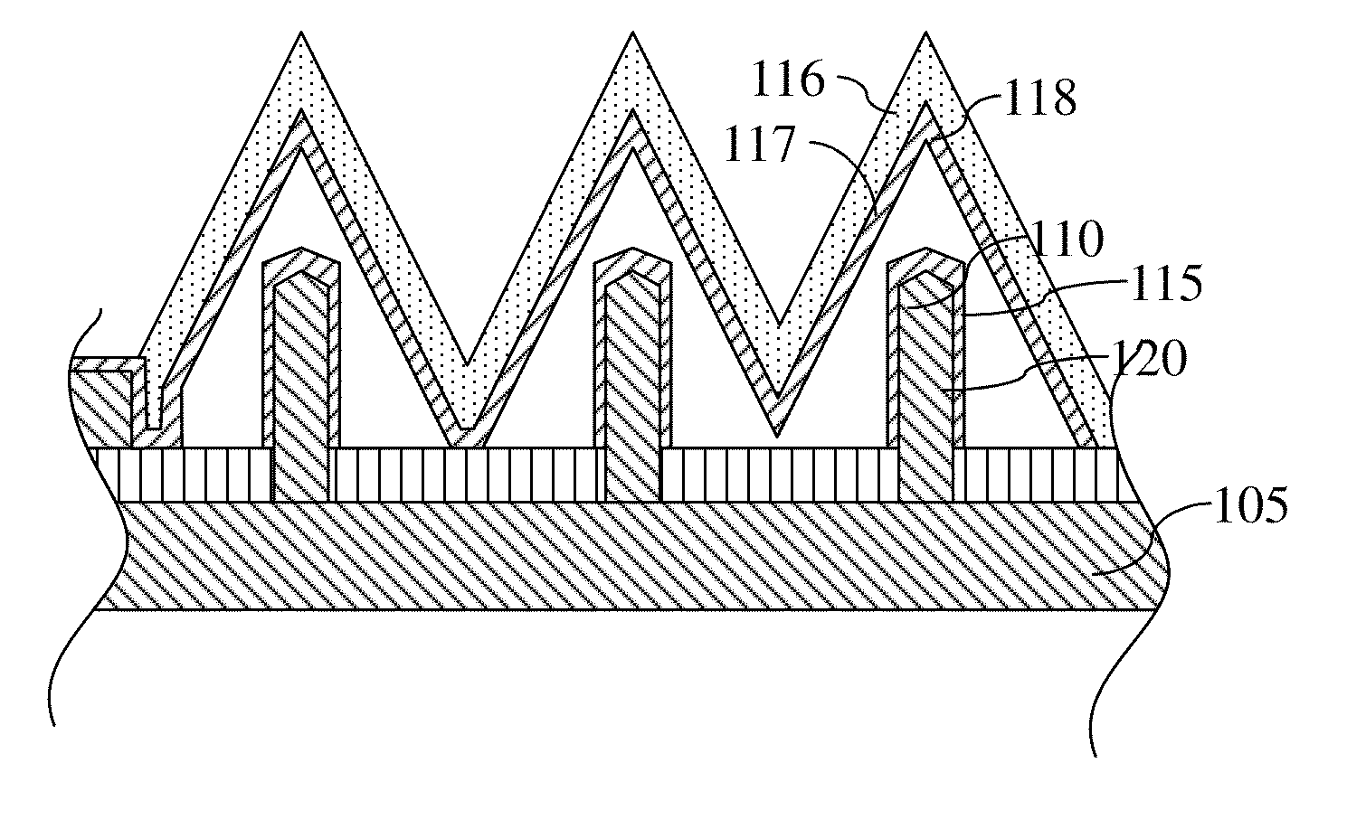

Image

  • Nitride nanowires and method of producing such
  • Nitride nanowires and method of producing such
  • Nitride nanowires and method of producing such

Examples


Embodiment Construction

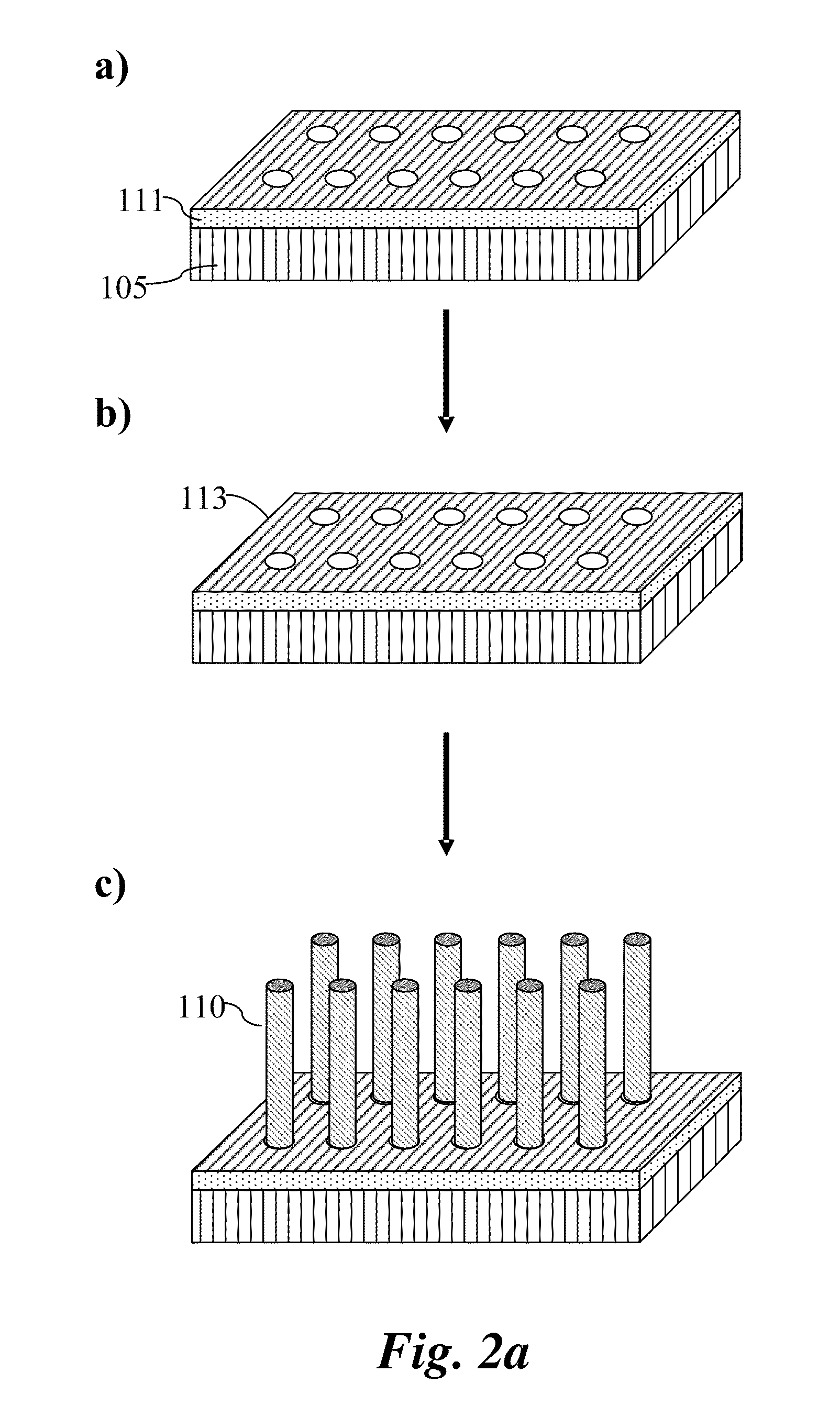
[0031]The semiconductor device and method to produce such according to the present invention comprises at least one nitride semiconductor nanowire, for example a GaN nanowire.

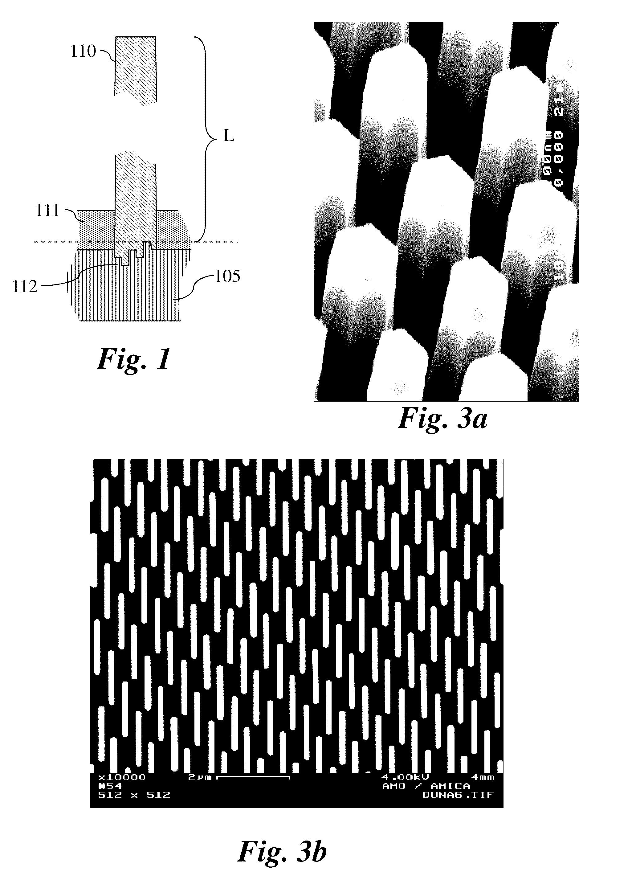
[0032]A nitride semiconductor nanowire 110, which is schematically illustrated in FIG. 1, is in this context defined as an essentially rod-shaped structure with a diameter less than 500 nm and a length up to several μm. The nanowire 110 is at its base epitaxially connected to a substrate 105, which may comprises of epitaxial layers, for example a layer of GaN closest to the nanowire 110. The nanowire 105 protrudes through an opening in a growth mask 111 of for example SiNx. A semiconductor device according to the invention typically comprises a plurality of nanowires 110. As indicated in FIG. 1 the surface of the substrate 105 may exhibit some roughness 112, exaggerated in the figure, for illustrative purposes only. Hereinafter the term nanowire should be understood as referring to the structure not restricted ...


PUM

PropertyMeasurementUnit
diameteraaaaaaaaaa
diameteraaaaaaaaaa
diameteraaaaaaaaaa

Abstract

The present invention relates to the growing of nitride semiconductors, applicable for a multitude of semiconductor devices such as diodes, LEDs and transistors. According to the method of the invention nitride semiconductor nanowires are grown utilizing a CVD based selective area growth technique. A nitrogen source and a metal-organic source are present during the nanowire growth step and at least the nitrogen source flow rate is continuous during the nanowire growth step. The V / III-ratio utilized in the inventive method is significantly lower than the V / III-ratios commonly associated with the growth of nitride based semiconductor.

Description

RELATED APPLICATIONS[0001]This application is a Continuation Application of co-pending U.S. Utility application Ser. No. 12 / 308,249, filed Dec. 11, 2008, the entire contents of which are hereby incorporated by reference.FIELD OF THE INVENTION[0002]The present invention relates to semiconductor devices based on nitride semiconductor nanowires and the method of producing such by the growing. Nitride semiconductor nanowires can be used as diodes, LEDs, LDs and transistors, for example. In particular the invention relates to a method of fabricating upstanding GaN nanowires with a limited lateral growth.BACKGROUND[0003]To use nitride semiconductors in semiconductor devices, in particular optoelectronic devices, has received considerable attention for a relatively long time not at least due to the potential possibility to achieve components active in wavelength areas not accessible with conventional semiconductor materials. In the 1990's, two breakthroughs have been made on nitride semico...

Claims


Application Information

Patent Timeline
Patent Type & Authority Applications(United States)
IPC IPC(8): H01L31/0256H01L31/0352
CPCB82Y10/00H01L33/24C30B29/406C30B29/60H01L21/02458H01L21/0254H01L21/02603H01L21/0262H01L21/02636H01L21/02639H01L29/0665H01L29/0673H01L29/0676H01L29/2003H01L33/007H01L33/06H01L33/18B82Y40/00H01L21/20C30B25/00Y10S977/932B82B1/00B82B3/00H01L33/0075H01L33/32H01L33/0093
Inventor SEIFERT, WERNERASOLI, DAMIRBI, ZHAOXIA
Owner QUNANO
Learn More