

Method of fabricating multi-level metallic parts by the liga-uv technique
a technology of multi-level metal parts, which is applied in the direction of 3d structure electroforming, coatings, instruments, etc., can solve the problems of inability to achieve an approximate flat top surface, inability to clean the room, and inability to meet the extreme cleanliness generally required for photolithography and galvanic deposition
- Summary
- Abstract
- Description
- Claims
- Application Information
AI Technical Summary
Benefits of technology
Problems solved by technology
Method used
Image

Examples
Embodiment Construction
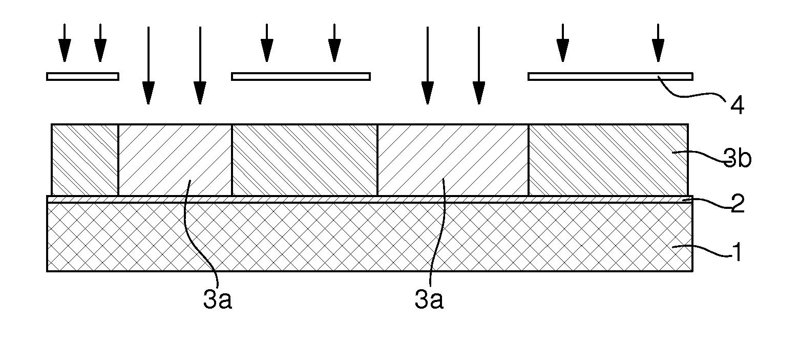
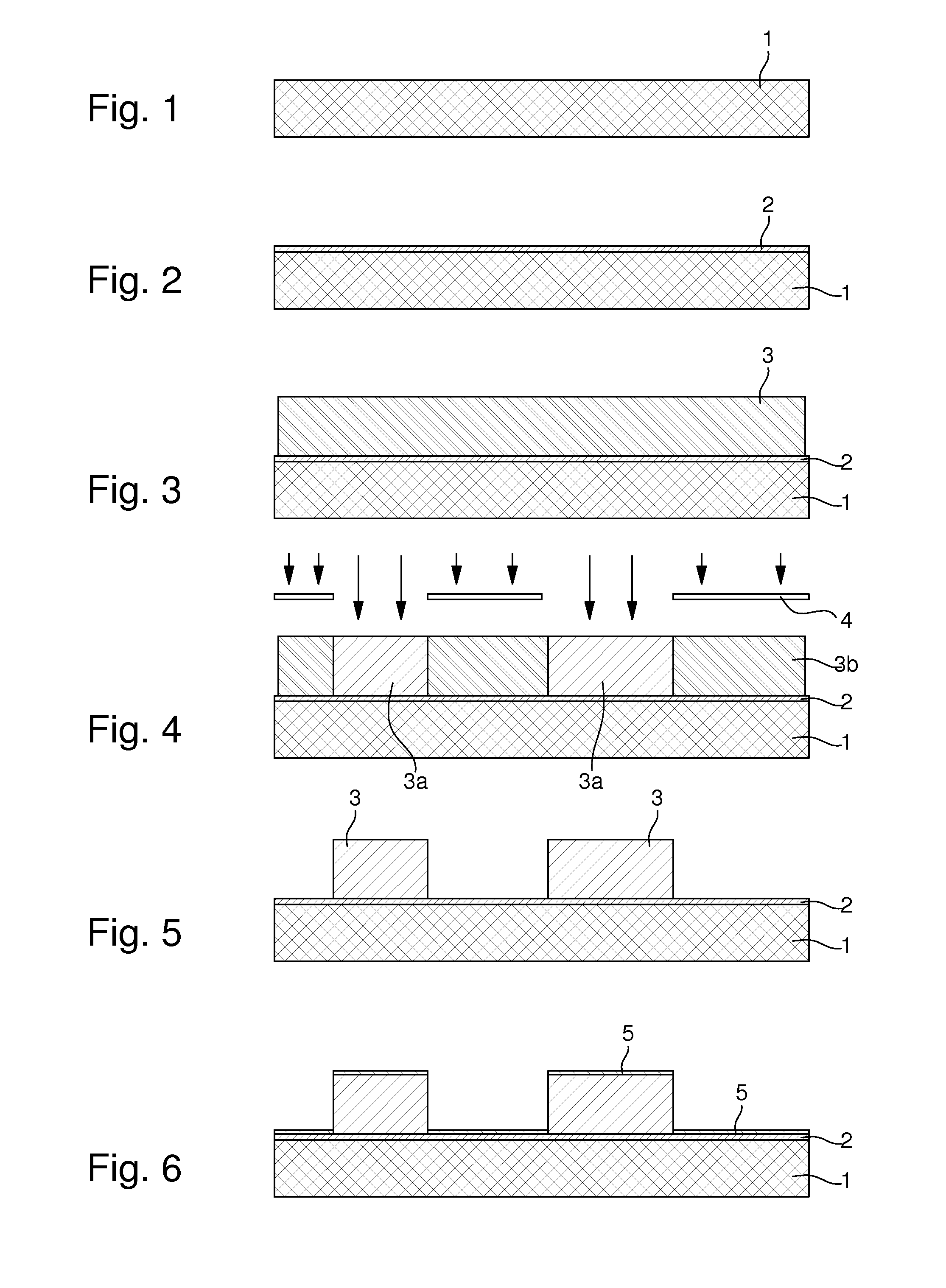
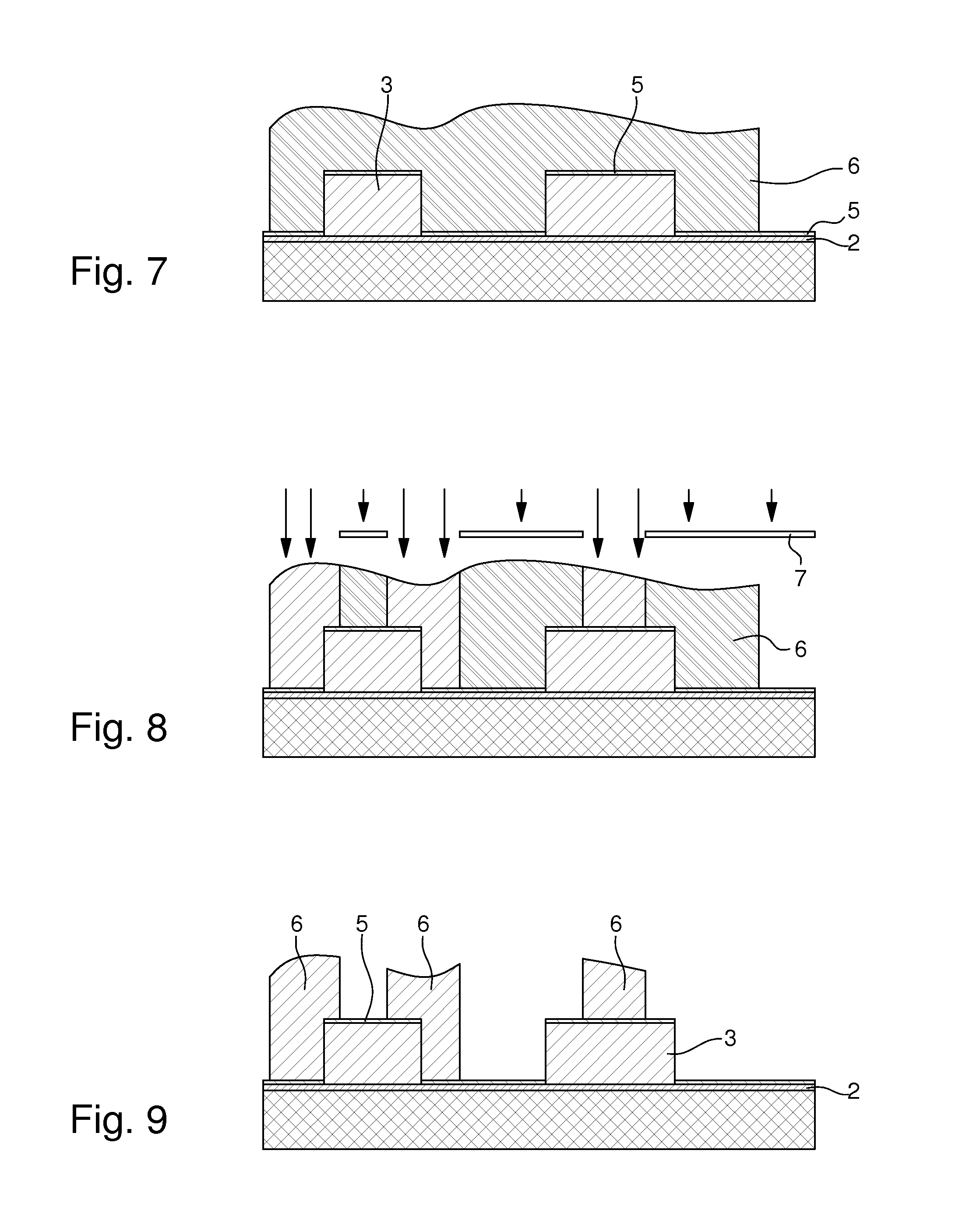
[0047]According to the present invention, the method includes the step of taking a substrate that has a conductive surface. In the particular implementation illustrated in the Figures, substrate 1 is formed by a silicon, glass or ceramic wafer (FIG. 1) on which a conductive layer 2 has been vapour-deposited (FIG. 2) beforehand. This conductive layer 2 is used as a priming layer, i.e. as a cathode, during a subsequent galvanic deposition. Typically, priming layer 2 can be formed of an underlayer of chromium or titanium covered with a gold or copper layer.
[0048]According to a variant that is not shown, prior to depositing priming layer 2, a sacrificial layer, which may, for example, be made of aluminium, is first of all vacuum plated on the substrate. The thickness of this layer is typically of the order of a tenth of a micron, and it is for enabling the multi-level metallic structure to be separated from the substrate at the end of the method. According to yet another variant, the sa...
PUM
| Property | Measurement | Unit |
|---|---|---|
| Electrical conductor | aaaaa | aaaaa |
| Photosensitivity | aaaaa | aaaaa |
Abstract
Description
Claims
Application Information