Semiconductor device

a technology of semiconductors and semiconductors, applied in the direction of transistors, basic electric elements, instruments, etc., to achieve the effects of reducing power consumption, ensuring stability, and ensuring reliability

Inactive Publication Date: 2011-06-23
SEMICON ENERGY LAB CO LTD
View PDF117 Cites 128 Cited by
  • Summary
  • Abstract
  • Description
  • Claims
  • Application Information

AI Technical Summary

Benefits of technology

[0021]Since the off current of a transistor including an oxide semiconductor is extremely low, stored data can be retained for an extremely long time by using the transistor. In other words, power consumption can be adequately reduced because refresh operation becomes unnecessary or the frequency of refresh operation can be extremely low. Moreover, stored data can be retained for a long time even when power is not supplied.
[0022]Further, high voltage is not needed to write data, and deterioration of the element does not become a problem. For example, since there is no need to perform injection of electrons to a floating gate or extraction of electrons from the floating gate which is needed in a conventional nonvolatile memory, a problem such as deterioration of a gate insulating layer does not occur. That is, the semiconductor device according to one embodiment of the present invention does not have a limit on the number of times of writing which is a problem in a conventional nonvolatile memory, and reliability thereof is drastically improved. Furthermore, data is written depending on the on state and the off state of the transistor, whereby high-speed operation can be easily realized. In addition, there is no need of operation for erasing data.

Problems solved by technology

A transistor formed using a highly-purified oxide semiconductor can retain data for a long time because leakage current thereof is extremely small.

Method used


Image

  • Semiconductor device
  • Semiconductor device
  • Semiconductor device

Examples


embodiment 1

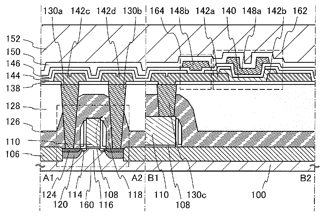
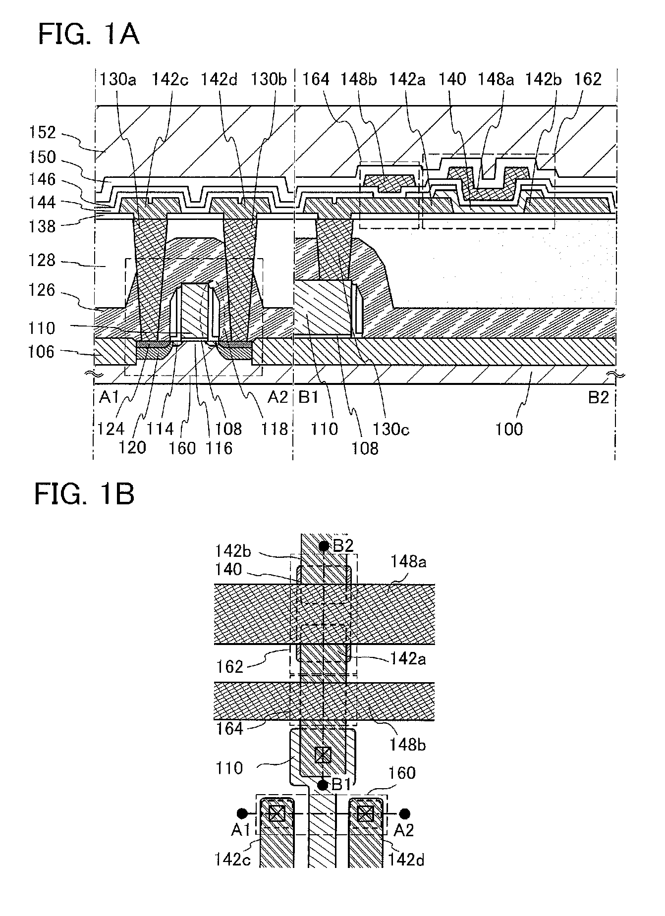
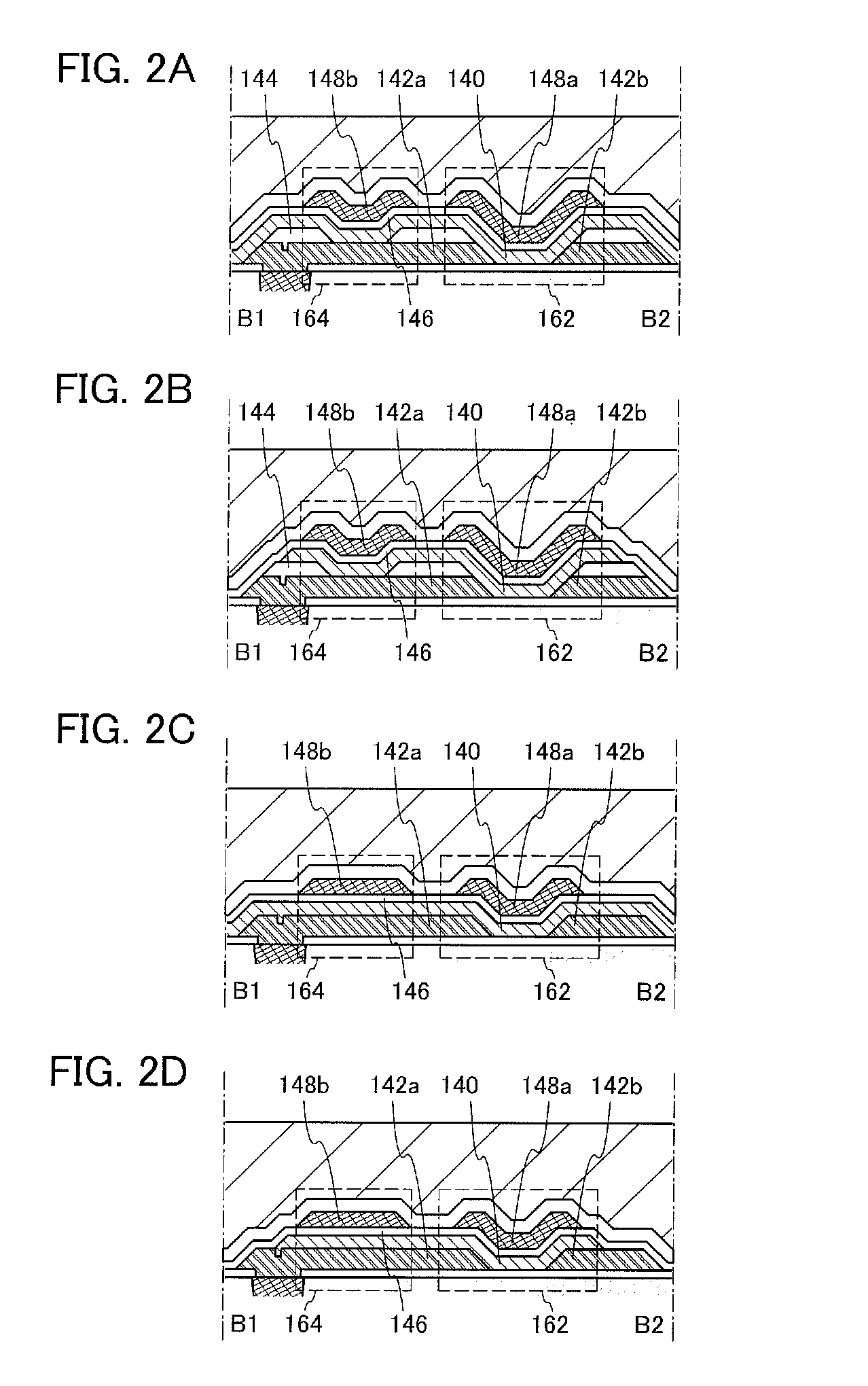
[0044]In this embodiment, a structure and a manufacturing method of a semiconductor device according to one embodiment of the invention disclosed is described with reference to FIGS. 1A and 1B, FIGS. 2A to 2D, FIGS. 3A1, A2, and 3B, FIGS. 4A to 4H, and FIGS. 5A to 5E. Note that in each of circuit diagrams, in some cases, “OS” is written beside a transistor in order to indicate that the transistor includes an oxide semiconductor.

[0045]FIGS. 1A and 1B illustrate an example of a structure of the semiconductor device. FIG. 1A illustrates a cross section of the semiconductor device, and FIG. 1B illustrates a plan view of the semiconductor device. Here, FIG. 1A corresponds to a cross section taken along lines A1-A2 and B1-B2 of FIG. 1B. In the semiconductor device illustrated in FIGS. 1A and 1B, a transistor 160 including a material other than an oxide semiconductor is provided in a lower portion, and a transistor 162 including an oxide semiconductor and a capacitor 164 are provided in an...

embodiment 2

[0165]In this embodiment, a semiconductor device which is different from that described in the above embodiment and a method for manufacturing a semiconductor device are described with reference to FIGS. 6A and 6B and FIGS. 7A to 7E. Note that the structure and the manufacturing process of the semiconductor device in this embodiment have a lot in common with those in Embodiment 1. Therefore, in the following description, repeated description of the same portions is omitted, and different points are described in detail.

[0166]FIGS. 6A and 6B illustrate an example of a structure of the semiconductor device. FIGS. 6A and 6B illustrate a cross section of the semiconductor device and a plan view thereof, respectively. Here, FIG. 6A corresponds to a cross section taken along line A3-A4 and line B3-B4 of FIG. 6B. In the semiconductor device illustrated in FIGS. 6A and 6B, in a similar manner to FIGS. 1A and 1B, a transistor 160 including a material other than an oxide semiconductor is inclu...

embodiment 3

[0175]In this embodiment, examples of a circuit configuration, operation, and the like of a semiconductor device which is formed using a plurality of semiconductor devices illustrated in Embodiment 1 are described with reference to FIGS. 8A and 8B and FIGS. 9A and 9B.

[0176]FIGS. 8A and 8B are examples of circuit diagrams of semiconductor devices each including a plurality of semiconductor devices (hereinafter also referred to as memory cells 190) illustrated in FIG. 3A1. FIG. 8A is a circuit diagram of a NAND semiconductor device in which the memory cells 190 are connected in series, and FIG. 8B is a circuit diagram of a NOR semiconductor device in which the memory cells 190 are connected in parallel.

[0177]The semiconductor device in FIG. 8A includes a source line SL, a bit line BL, a first signal lines S1, a plurality of second signal lines S2, a plurality of word lines WL, and the plurality of memory cells 190. In each of the memory cells 190, a gate electrode of the transistor 16...


PUM


Abstract

A first transistor including a channel formation region, a first gate insulating layer, a first gate electrode, and a first source electrode and a first drain electrode; a second transistor including an oxide semiconductor layer, a second source electrode and a second drain electrode, a second gate insulating layer, and a second gate electrode; and a capacitor including one of the second source electrode and the second drain electrode, the second gate insulating layer, and an electrode provided to overlap with one of the second source electrode and the second drain electrode over the second gate insulating layer are provided. The first gate electrode and one of the second source electrode and the second drain electrode are electrically connected to each other.

Description

TECHNICAL FIELD[0001]The invention disclosed herein relates to a semiconductor device including a semiconductor element and a method for manufacturing the semiconductor device.BACKGROUND ART[0002]Storage devices using semiconductor elements are broadly classified into two categories: a volatile device that loses stored data when power supply stops, and a non-volatile device that retains stored data even when power is not supplied.[0003]A typical example of a volatile storage device is a DRAM (dynamic random access memory). A DRAM stores data in such a manner that a transistor included in a storage element is selected and electric charge is stored in a capacitor.[0004]When data is read from a DRAM, charge in a capacitor is lost on the above-described principle; thus, another writing operation is necessary every time data is read out. Moreover, a transistor included in a storage element has a leakage current and electric charge flows into or out of a capacitor even when the transistor...

Claims


Application Information

Patent Timeline
Patent Type & Authority Applications(United States)
IPC IPC(8): H01L29/12
CPCG11C16/0416H01L21/28518H01L27/11517H01L27/1156H01L27/1207H01L29/7869H01L28/40H01L29/6659H01L27/10855H01L27/10805H01L27/1225H10B41/30H01L2924/0002H10B41/00H10B41/70H01L2924/00H10B12/30H10B69/00H10B12/0335H01L23/528H01L27/1255H01L29/24H01L29/78
Inventor YAMAZAKI, SHUNPEIKOYAMA, JUNKATO, KIYOSHI
Owner SEMICON ENERGY LAB CO LTD
Why Eureka
Try Eureka