Bipolar Transistor with Pseudo Buried Layers

a bipolar transistor and pseudo-buried layer technology, applied in the direction of semiconductor devices, basic electric elements, electrical equipment, etc., can solve the problems of not meeting the rf requirement, the advanced cmos process is quite expensive, and the cost of materials, etc., to achieve less parasitic effect, less device size, and less photo mask layer

Inactive Publication Date: 2011-06-23
SHANGHAI HUA HONG NEC ELECTRONICS
View PDF6 Cites 23 Cited by
  • Summary
  • Abstract
  • Description
  • Claims
  • Application Information

AI Technical Summary

Benefits of technology

[0010]The invention of bipolar transistor omits conventional collector buried layer process, collector epitaxial growth and heavily doped collector pick-up. Instead the pseudo buried layers implanted at the bottoms of shallow trenches are taken as buried layers, the collector area is formed by implantations, and the deep trench contacts in field oxide are used for collector pick-up. Compared to conventional bipolar transistors, the bipolar transistor in present invention has smaller device size, less parasitic effect, fewer photo mask layers and lower process cost.

Problems solved by technology

However RFCMOS still cannot satisfy RF requirement ((Ft higher than 40 GHz), and further more, advanced CMOS process is quite expensive.
The compound semiconductor devices can achieve very high Ft, while their expensive materials, small size substrate and material poisonousness limit their applications.
However it has some disadvantages: 1. too expensive for collector epitaxy; 2. Collector pick-up is formed by high dose, high energy implant.
Its occupied area is large; 3. Deep trench isolation process is complicated and expensive; 4. There are too many photo mask layer to fabricate transistors.

Method used


Image

  • Bipolar Transistor with Pseudo Buried Layers
  • Bipolar Transistor with Pseudo Buried Layers
  • Bipolar Transistor with Pseudo Buried Layers

Examples


Embodiment Construction

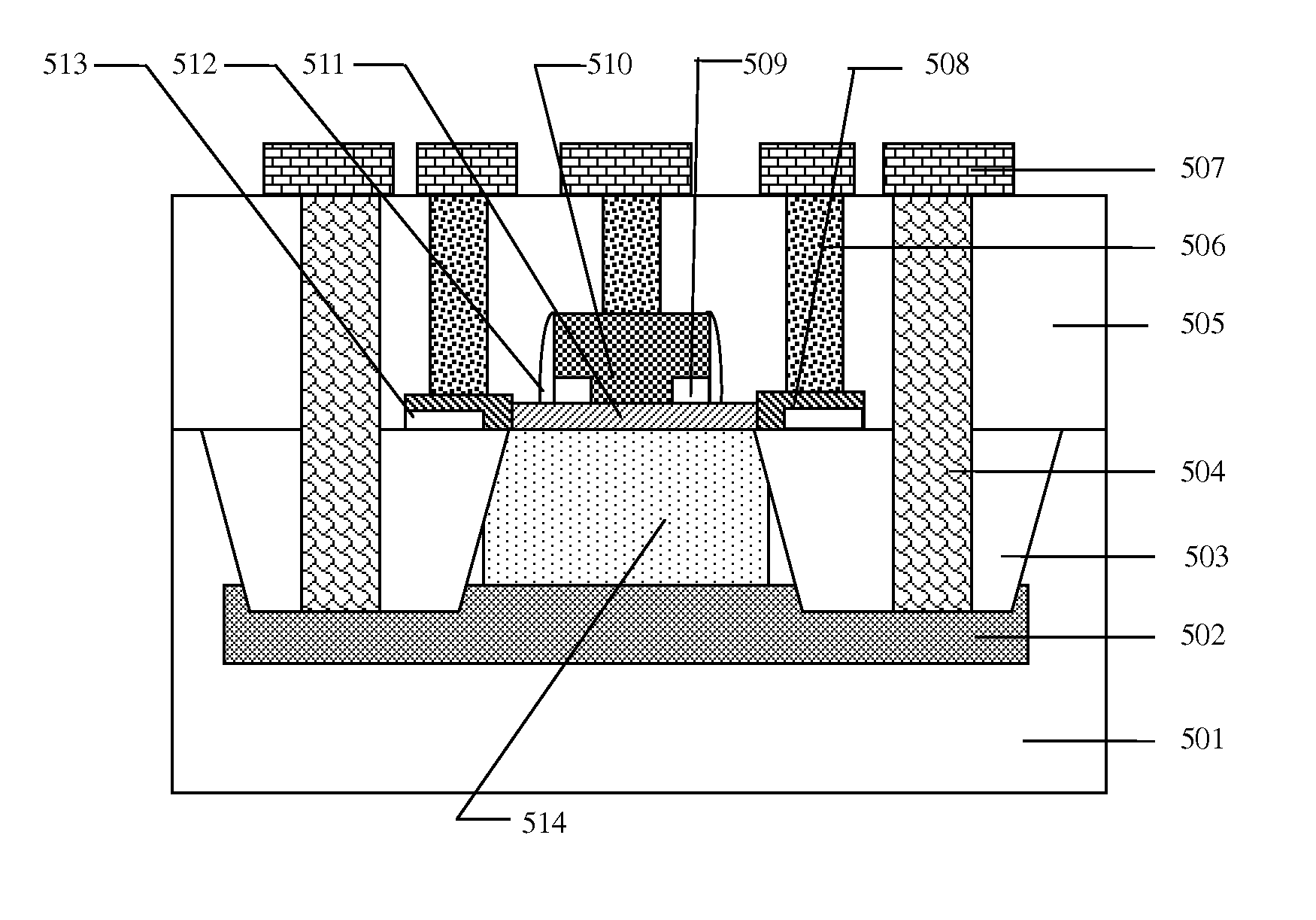
[0018]FIG. 2 is cross sectional view showing the structure of the bipolar transistors in the invention. On substrate 501, the active area is isolated by field oxide 503 in shallow trenches. The transistor comprises a collector 514, a base 511 and an emitter 510.

[0019]The collector 514 is formed by single or multiple implants of first electric type impurity into active area. At the bottom of collector 514, two pseudo buried layers 502 at STI bottoms link up to be buried layer. For active critical dimension less than 0.5 micron, two pseudo buried layers 502 overlap in active by lateral diffusion and become collector 514's buried layer. If active critical dimension is larger than 0.5 micron, the implant into active with the same impurity type as pseudo buried layer 502 is implemented to link two pseudo buried layers. The implant depth is almost same as that of pseudo buried layers. The deep trench contacts 504 are etched through the field oxide 503 above pseudo buried layers 502 to con...


PUM


Abstract

A structure and fabrication method for a bipolar transistor with shallow trench isolation (STI) comprises a collector formed by implanting first electric type impurity in active area; pseudo buried layers at the bottom of STI at both sides of active area by implanting heavy dose of first electric type impurity; deep contacts through field oxide to connect to pseudo buried layers and to pick up the collector; a base, a thin film deposited on the collector and doped with second electric type impurity; an emitter, a polysilicon film doped by heavy dose implant of first electric type impurity. This transistor has smaller device area, less parasitic effect, less photo layers and lower process cost.

Description

[0001]The current application claims a foreign priority to an application in China with a serial number 200910202011.7 filed on Dec. 21, 2009.FIELD OF THE INVENTION[0002]This invention relates generally to semiconductor devices in integrated circuits. More particularly it relates to bipolar transistor design and fabrication.BACKGROUND OF THE INVENTION[0003]In radio frequency (RF) applications, higher and higher cut-off frequency (Ft) of RF transistor is required. RFCMOS with advanced technology nodes can realize high cut-off frequency. However RFCMOS still cannot satisfy RF requirement ((Ft higher than 40 GHz), and further more, advanced CMOS process is quite expensive. The compound semiconductor devices can achieve very high Ft, while their expensive materials, small size substrate and material poisonousness limit their applications. Silicon bipolar junction transistor (BJT) and SiGe hetrojunction bipolar transistor (HBT) are the best options of high Ft devices.[0004]NPN transistor...

Claims


Application Information

Patent Timeline
Patent Type & Authority Applications(United States)
IPC IPC(8): H01L29/70H01L21/331
CPCH01L21/76232H01L29/0821H01L29/732H01L29/66287H01L29/41708
Inventor CHIU, TZUYINCHU, TUNGYUANQIAN, WENSHENGFAN, YUNGCHIEH
Owner SHANGHAI HUA HONG NEC ELECTRONICS
Why Eureka
Try Eureka