Semiconductor device and method of fabricating the same

a technology of semiconductors and components, applied in the direction of semiconductor devices, basic electric elements, electrical appliances, etc., can solve the problems of deterioration of refresh characteristics of drams, increased junction leakage,

Inactive Publication Date: 2011-06-23
ELPIDA MEMORY INC
View PDF10 Cites 3 Cited by
  • Summary
  • Abstract
  • Description
  • Claims
  • Application Information

AI Technical Summary

Benefits of technology

[0007]In one embodiment, a method of forming a semiconductor device may include, but is not limited to the following processes. A groove is formed in a semiconductor substrate. A gate electrode is formed in the groove. A...

Problems solved by technology

Also, when the concentration of a substrate is increased to suppress a drop in threshold voltage V...

Method used


Image

  • Semiconductor device and method of fabricating the same
  • Semiconductor device and method of fabricating the same
  • Semiconductor device and method of fabricating the same

Examples


Embodiment Construction

[0069]Before describing the present invention, the related art will be explained in detail, with reference to drawings, in order to facilitate the understanding of the present invention.

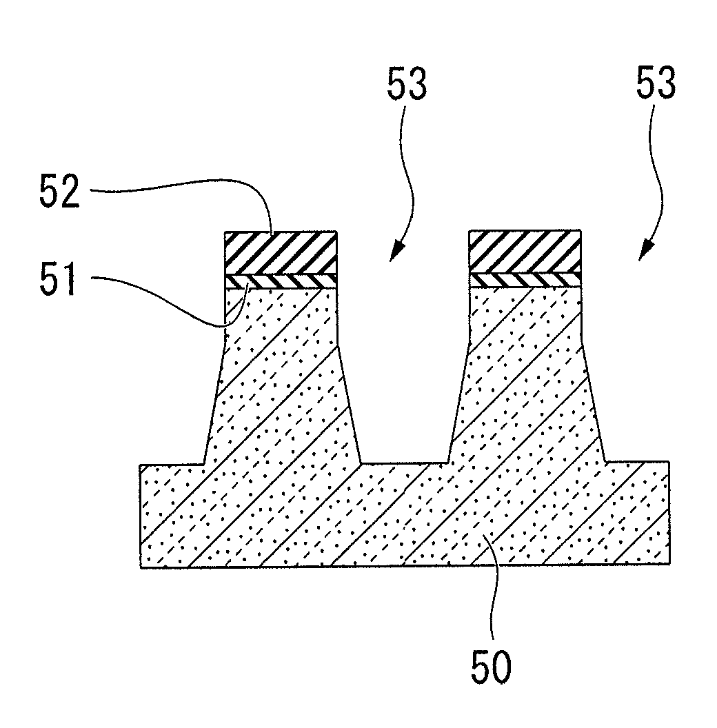
[0070]FIG. 29 is a schematic cross-sectional view showing an example of a structure of a DRAM including a trench-gate cell transistor. In a DRAM 200 having the structure shown in FIG. 29, element isolation regions 202 are formed in a surface of a P-type silicon substrate 201 and spaced apart from each other from side to side. Gate trenches 204 are formed in a region of the semiconductor substrate 201 interposed between the element isolation regions 202 and spaced apart from each other in a lateral direction of FIG. 33. Gate electrodes 212 are formed to fill the gate trenches 204 through a gate insulating film 205 formed on inner walls of the gate trenches 204 between the gate electrodes 212 and the gate trenches 204.

[0071]The gate electrodes 212 fill the gate trenches 204 and simultaneously protrude ...


PUM


Abstract

A method of forming a semiconductor device, the method including the following processes. A groove is formed in a semiconductor substrate. A gate electrode is formed in the groove. A boron-phosphorus silicate glass film is formed over the gate electrode. An etching process is performed using the boron-phosphorus silicate glass film as an etching stopper for preventing the gate electrode from being removed.

Description

BACKGROUND OF THE INVENTION[0001]1. Field of the Invention[0002]The present invention relates to a semiconductor device and a method of fabricating the same.[0003]Priority is claimed on Japanese Patent Application No. 2009-287801, Dec. 18, 2009, the content of which is incorporated herein by reference.[0004]2. Description of the Related Art[0005]In recent years, the miniaturization of dynamic random access memory (DRAM) cells has necessitated a reduction in gate length of an access transistor (hereinafter, referred to as a “cell transistor”) of a cell array. However, as the gate length of the cell transistor decreases, a short channel effect of the cell transistor increases. Thus, the threshold voltage Vt of the cell transistor is reduced due to an increase in subthreshold current. Also, when the concentration of a substrate is increased to suppress a drop in threshold voltage Vt, junction leakage increases. As a result, deterioration of refresh characteristics of a DRAM may occur.[...

Claims


Application Information

Patent Timeline
IPC IPC(8): H01L21/28
CPCH01L27/10814H01L27/10855H01L29/4236H01L27/10891H01L27/10876H10B12/315H10B12/0335H10B12/053H10B12/488
Inventor FUKUSHIMA, YOICHI
Owner ELPIDA MEMORY INC
Why Eureka
Try Eureka