

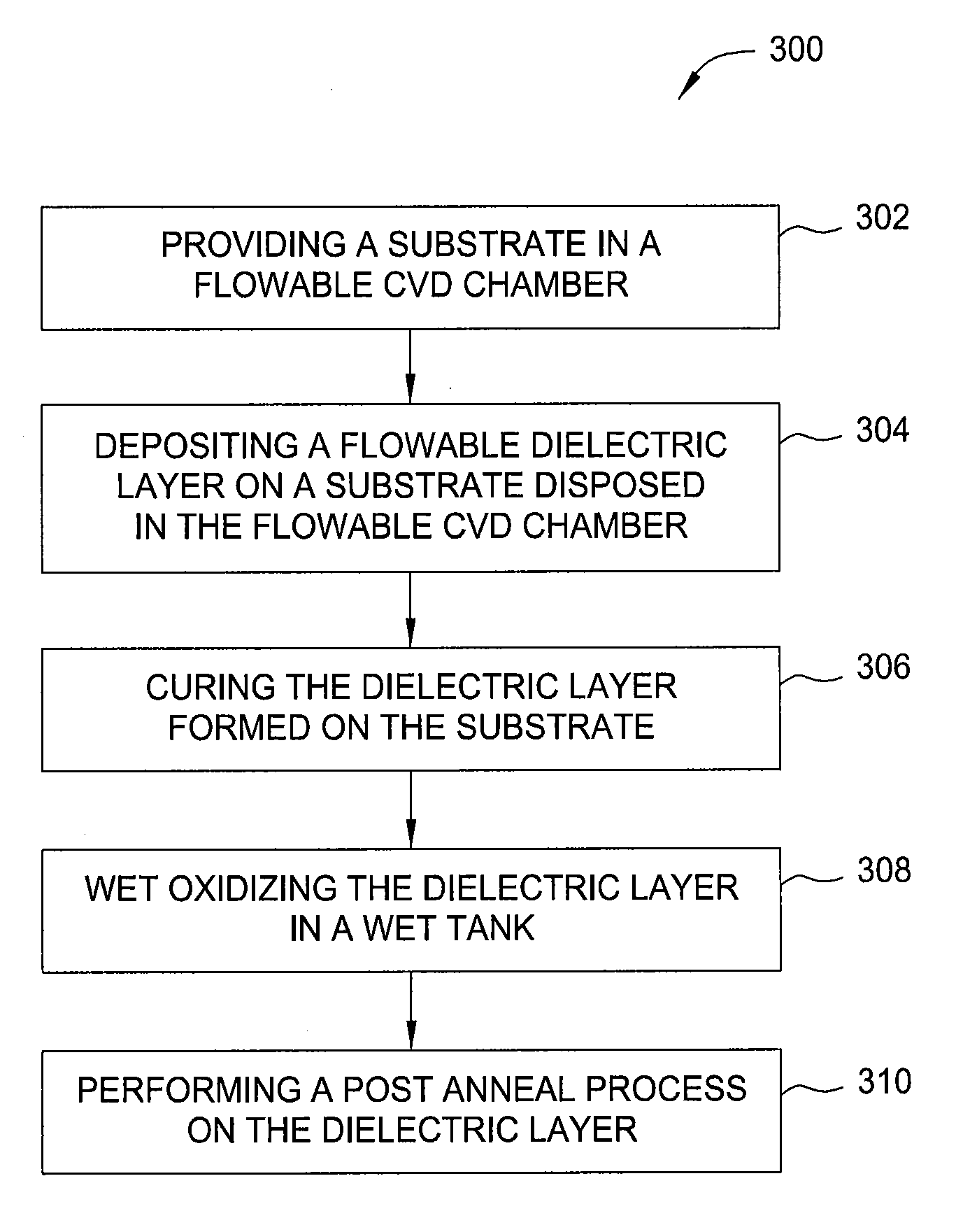
Wet oxidation process performed on a dielectric material formed from a flowable CVD process
- Summary
- Abstract
- Description
- Claims
- Application Information
AI Technical Summary
Benefits of technology
Problems solved by technology
Method used
Image

Examples
Embodiment Construction
nd
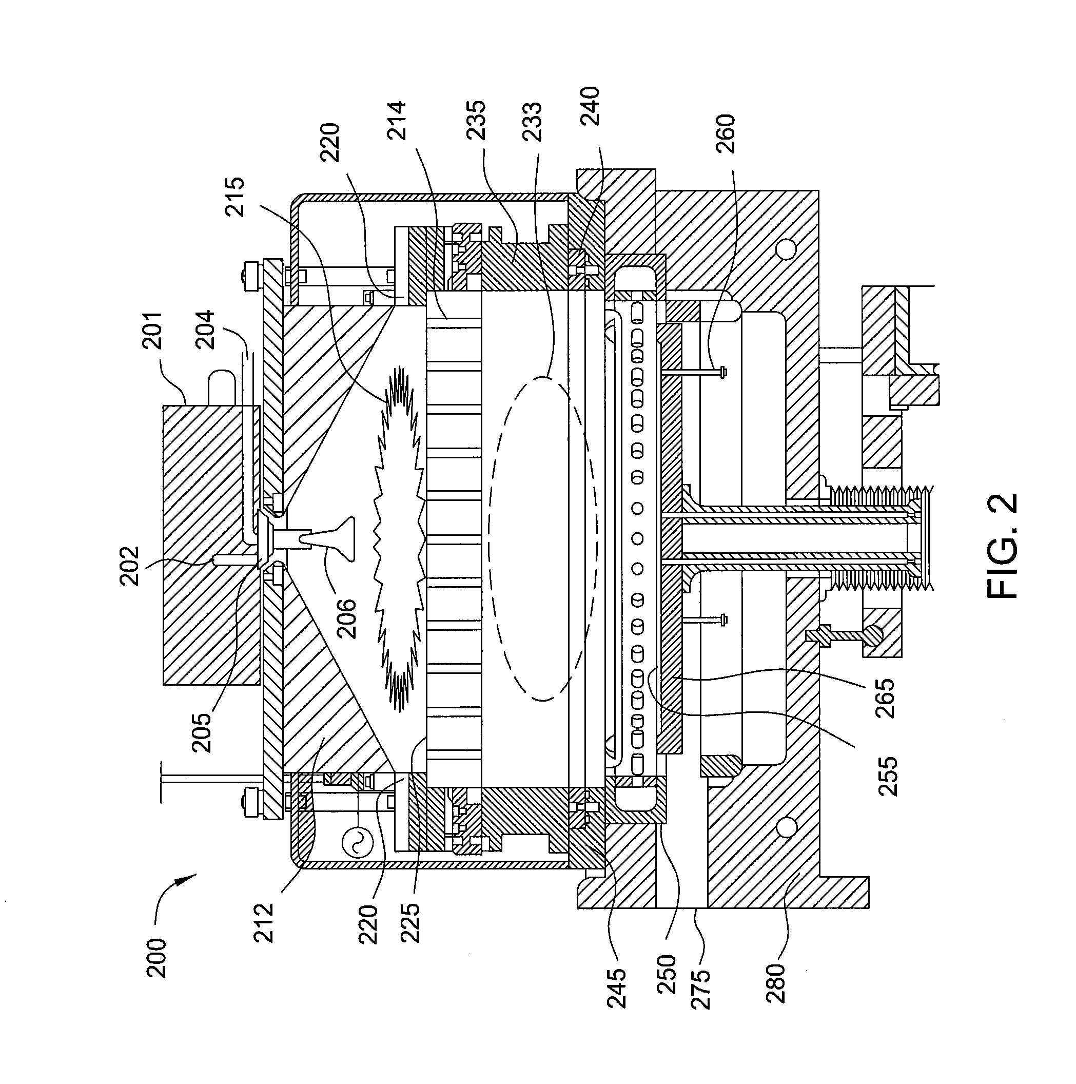
[0019]FIG. 5 is a schematic cross-sectional view of a wet process tank that may be used according to one embodiment of the invention.
[0020]To facilitate understanding, identical reference numerals have been used, where possible, to designate identical elements that are common to the figures. It is also contemplated that elements disclosed in one embodiment may be beneficially utilized on other embodiments without specific recitation.
DETAILED DESCRIPTION
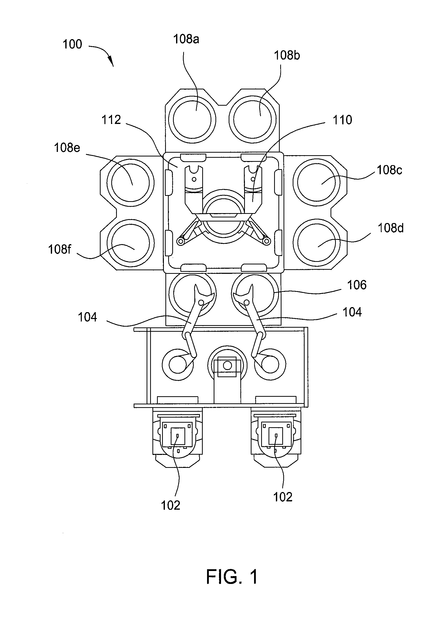
[0021]FIG. 1 is a top plan view of one embodiment of a processing tool 100 of deposition, baking and curing chambers according to disclosed embodiments. In the processing tool 100, a pair of FOUPs (front opening unified pods) 102 supply substrate substrates (e.g., 300 mm diameter wafers) that are received by robotic arms 104 and placed into load lock chambers 106. A second robotic arm 110 is disposed in a transfer chamber 112 coupled to the load lock chambers 106. The second robotic arm 110 is used to transport the substrates from t...
PUM
 Abstract
Description
Claims
Application Information