Supercharge Your Innovation With Domain-Expert AI Agents!

Interface apparatus for semiconductor integrated circuit and interfacing method thereof

a technology of integrated circuits and interface apparatuses, applied in the direction of logic circuit coupling/interface arrangements, single output arrangements, pulse techniques, etc., can solve the problems of complex interpolation and oversampling processes that are too complicated to be simply realized in the output block, and may occur bit errors

Active Publication Date: 2011-06-30
SK HYNIX INC
View PDF8 Cites 2 Cited by
  • Summary
  • Abstract
  • Description
  • Claims
  • Application Information

AI Technical Summary

Benefits of technology

[0044]According to the first embodiment of the present invention, outputting the signal IN and bar signal INB with their VOX controlled to the target level improves the reliability of an interface apparatus of a semiconductor integrated circuit.

Problems solved by technology

When a voltage level VOX of a signal and a bar signal outputted by the output block are outside of a set range, a bit error may occur in an input block of an external circuit.
Since no conventional technology provides a method for directly detecting the VOX, the VOX is indirectly detected by detecting jitter.
When the VOX is converted into a time domain, it becomes jitter, and the fact that the cross point of a signal and a bar signal between a power source voltage VDD and a ground voltage VSS varies with a swing level indicates that a timing error has occurred.
However, the conventional technologies have a drawback in that the interpolation and oversampling processes are too complicated to be simply realized in the output block.
Moreover, since the output block characteristically occupies a large volume and since it includes a circuit having a high power consumption, the output path through which a data is outputted by the output block to an external circuit takes less time than an input path through which data is inputted from the input block to the internal circuitry of an integrated circuit.
Therefore, it is difficult to add a circuit requiring a delay.

Method used


Image

  • Interface apparatus for semiconductor integrated circuit and interfacing method thereof
  • Interface apparatus for semiconductor integrated circuit and interfacing method thereof
  • Interface apparatus for semiconductor integrated circuit and interfacing method thereof

Examples


first embodiment

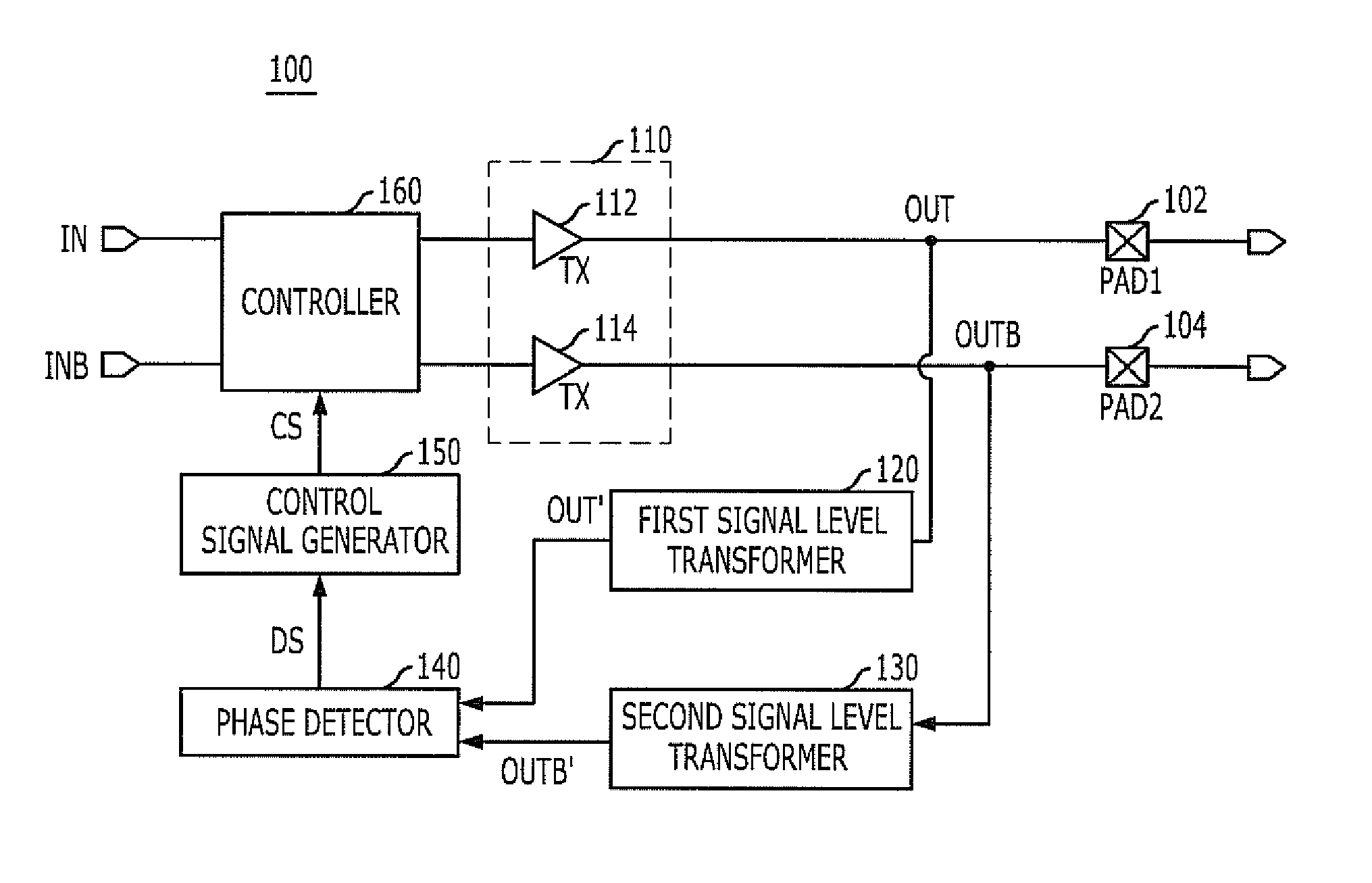
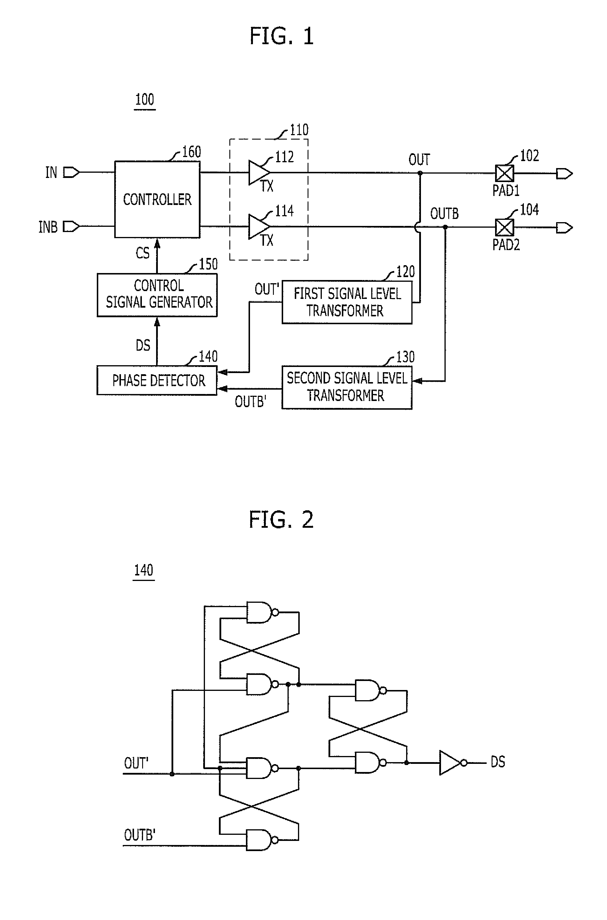
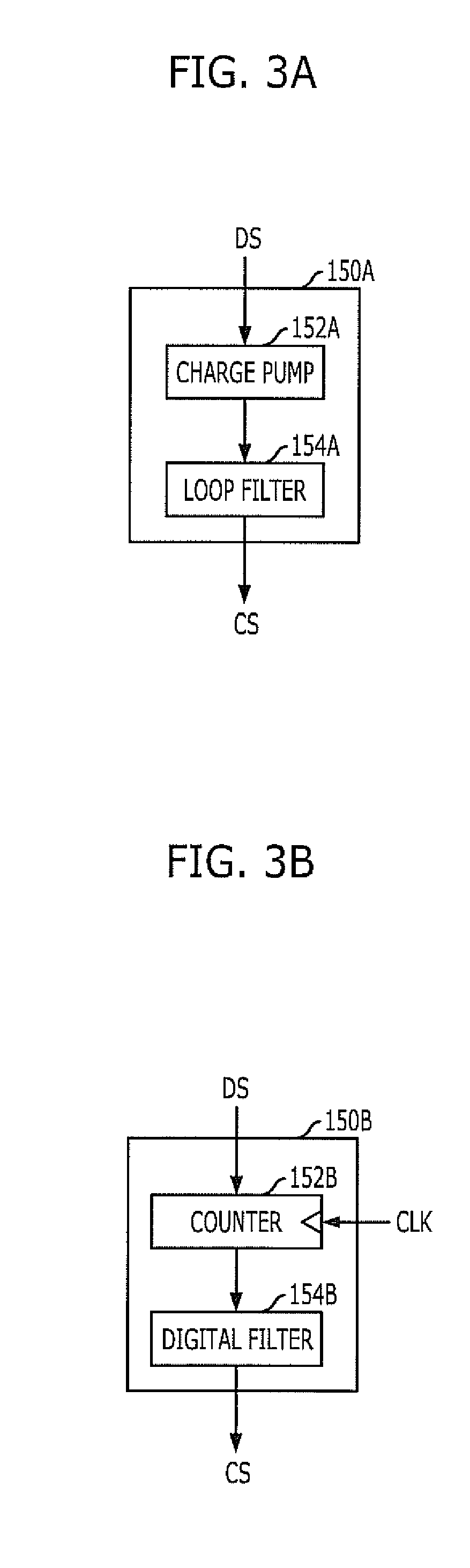
[0026]FIG. 1 is a block diagram illustrating an interface apparatus for a semiconductor integrated circuit in accordance with the present invention. FIG. 2 illustrates a phase detector shown in FIG. 1. FIGS. 3A to 3C are block diagrams describing an analog control signal generator and two digital control signal generators. FIGS. 4A and 4B illustrate a controller shown in FIG. 1 along with a first output buffer.

[0027]In the first embodiment, a one-directional interface apparatus including an output block has been selected as an example and is described as follows. Referring to FIG. 1, an interface apparatus 100 provided within a semiconductor integrated circuit (IC) includes an output block 110, which buffers a signal IN and a bar signal INB generated by an internal circuit (not shown) of the semiconductor integrated circuit and outputs the buffered signals to an external circuit (not shown) through a first pad 102 (PAD1) and a second pad 104 (PAD2). The output block 110 includes a f...

second embodiment

[0052]Hereafter, an operation of the interface apparatus in accordance with the present invention is described below, referring to FIG. 8.

[0053]FIG. 8 is a flowchart illustrating an interfacing method of the interface apparatus in accordance with the second embodiment of the present invention.

[0054]Herein, it is assumed in the description of the second embodiment that controlling VOX corresponds to controlling a time delay.

[0055]Referring to FIG. 8, in step S210, an output block 210 is enabled by an output enable signal EN. In step S202, the output block 210 begins to be driven and enters into an output stand-by state and at the same time a first switch 232 and a second switch 234 are controlled to be open. Since the first switch 232 and the second switch 234 are open, an input block 220 is switched from an input stand-by state to a feedback stand-by state.

[0056]When a signal IN and a bar signal INB output by an internal circuit of a semiconductor integrated circuit are transferred ...

third embodiment

[0062]FIG. 9 is a block diagram illustrating an interface apparatus of a semiconductor integrated circuit in accordance with the present invention. FIG. 10 is a circuit diagram illustrating an output controller shown in FIG. 9. For the sake of convenience in description, only a line for a signal IN is illustrated in FIG. 10.

[0063]The third embodiment of the present invention is designed to control a slew of a signal and a bar signal generated by an internal circuit of a semiconductor integrated circuit. The interface apparatus in accordance with the third embodiment of the present invention may be applied to both a one-directional interface apparatus and a bi-directional interface apparatus. The same reference numerals are given to the same constituent elements as those shown in the first embodiment and a description on the same constituent elements has been omitted herein.

[0064]Referring to FIGS. 9 and 10, the interface apparatus 100′ includes a timing control and output block 110′...


PUM


Abstract

An interface apparatus for a semiconductor integrated circuit and an interfacing method thereof controls the VOX of differential signals to a target level in response to the differential signals being outputted by an output block. The interface apparatus for a semiconductor integrated circuit includes an output block configured to output differential signals output by an internal circuit a detector configured to detect a timing error of the differential signals; and a controller configured to control a timing of the differential signals output by the internal circuit according to a detection result of the detector.

Description

CROSS-REFERENCE TO RELATED APPLICATION[0001]The present application claims priority of Korean Patent Application No. 10-2009-0133391, filed on Dec. 29, 2009, which is incorporated herein by reference in its entirety.BACKGROUND OF THE INVENTION[0002]Exemplary embodiments of the present invention relate to a semiconductor integrated circuit, and more particularly, to an interface apparatus of a semiconductor integrated circuit and an interfacing method thereof.[0003]Recently designed semiconductor integrated circuits (ICs) require a high degree of integration, low power consumption, and a high operating speed. To fulfill these requirements, semiconductor integrated circuits are equipped with an interface apparatus for transmitting / receiving a signal / bar signal to / from an external circuit. Herein, the signal / bar signal includes a data signal and a data bar signal (that is, a logically inverted data signal), an address signal and an address bar signal (that is, a logically inverted addr...

Claims


Application Information

Patent Timeline
IPC IPC(8): H03L7/06
CPCH03K19/0175H03K5/1565
Inventor LEE, JI-WANGKIM, YONG-JUSONG, HEE-WOONGOH, IC-SUKIM, HYUNG-SOOWANG, TAE-JINCHOI, HAE-RANGJANG, JAE-MINPARK, CHANG-KUN
Owner SK HYNIX INC
Features
  • R&D
  • Intellectual Property
  • Life Sciences
  • Materials
  • Tech Scout
  • Unparalleled Data Quality
  • Higher Quality Content
  • 60% Fewer Hallucinations
Learn More