Memory Cell Using Leakage Current Storage Mechanism

a leakage current and storage mechanism technology, applied in the field of memory cells, can solve the problems of increased leakage current, no useful purpose in most conventional ics, and leakage current within, and achieve the effect of enhancing the stability of four-transistor memory cells and less susceptibl

Inactive Publication Date: 2011-06-30
LSI CORPORATION
View PDF3 Cites 17 Cited by
  • Summary
  • Abstract
  • Description
  • Claims
  • Application Information

AI Technical Summary

Benefits of technology

xpensive to operate. An additional advantage of the invention includes, for example, enhanced four-transistor memory cell stability due to maintaining stored data by active current on at least one storage node of the four-transistor memory cell, regardless of the data state being stored therein. This results in a more robust memory cell design which is significantly less susceptible to noise and other undesirable memory disturbs compared to conventional memory cells.
These and other features, objects and advantages of the present invention will become apparent from the following detailed description of illustrative embodiments thereof, which is to be read in connection with the accompanying drawings.

Problems solved by technology

Leakage power is proportional to leakage current and, typically, serves no useful purpose in most conventional ICs.
In recent IC fabrication technologies, leakage currents have increased and become a critical concern.
As a result, a major component of leakage current within an IC is attributable to leakage current within the individual memory cells.
Unfortunately, reducing the geometry of the memory cells often results in increased leakage current in the cells, which has been conventionally disadvantageous.

Method used


Image

  • Memory Cell Using Leakage Current Storage Mechanism
  • Memory Cell Using Leakage Current Storage Mechanism
  • Memory Cell Using Leakage Current Storage Mechanism

Examples


Embodiment Construction

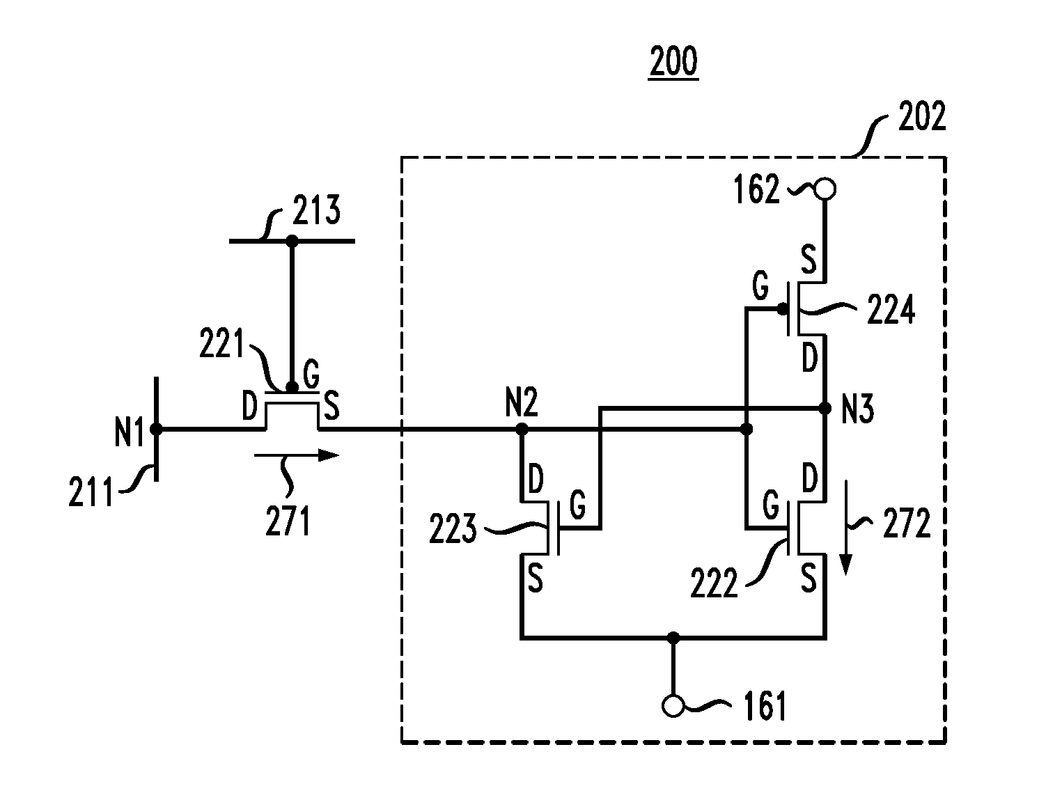
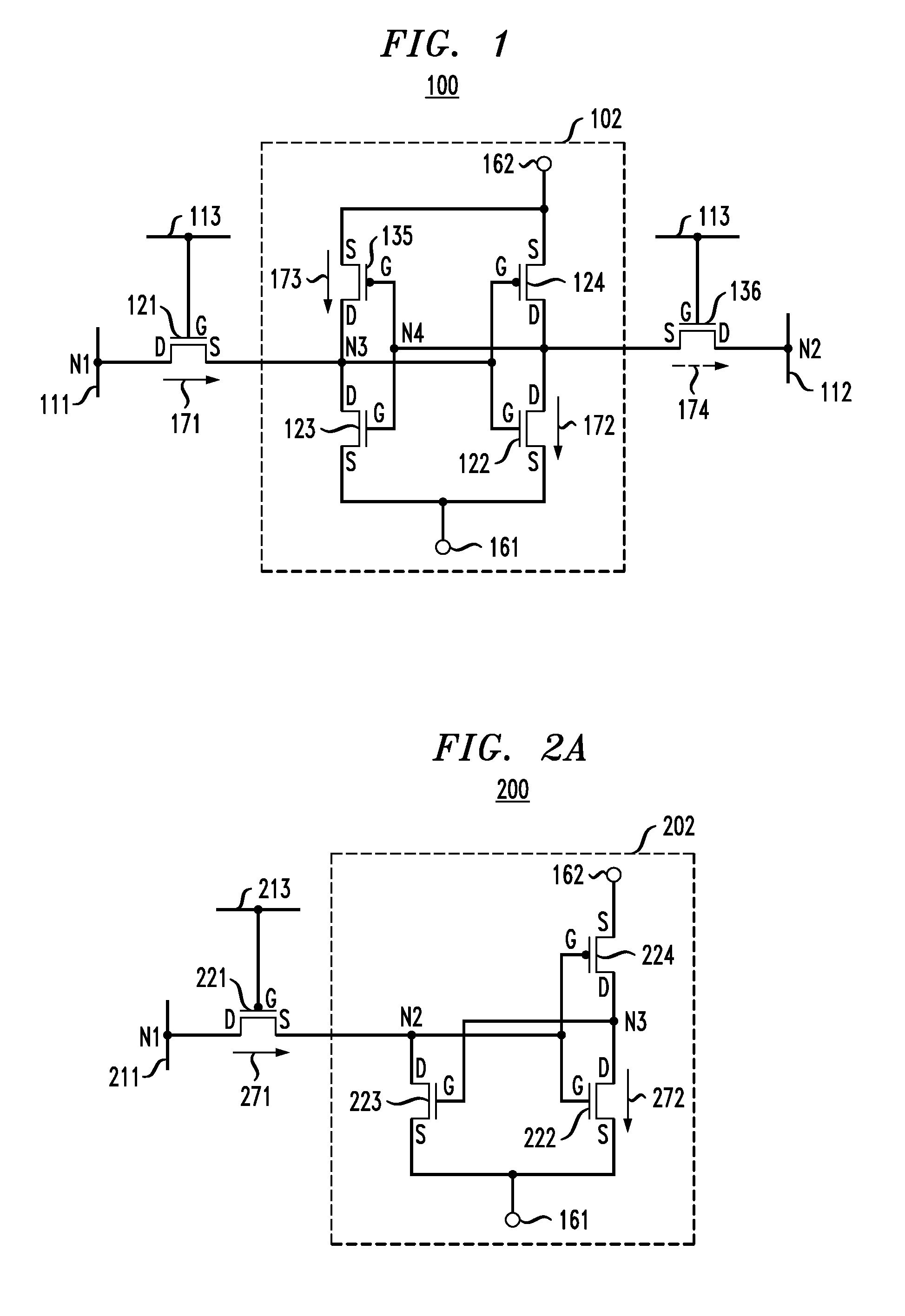
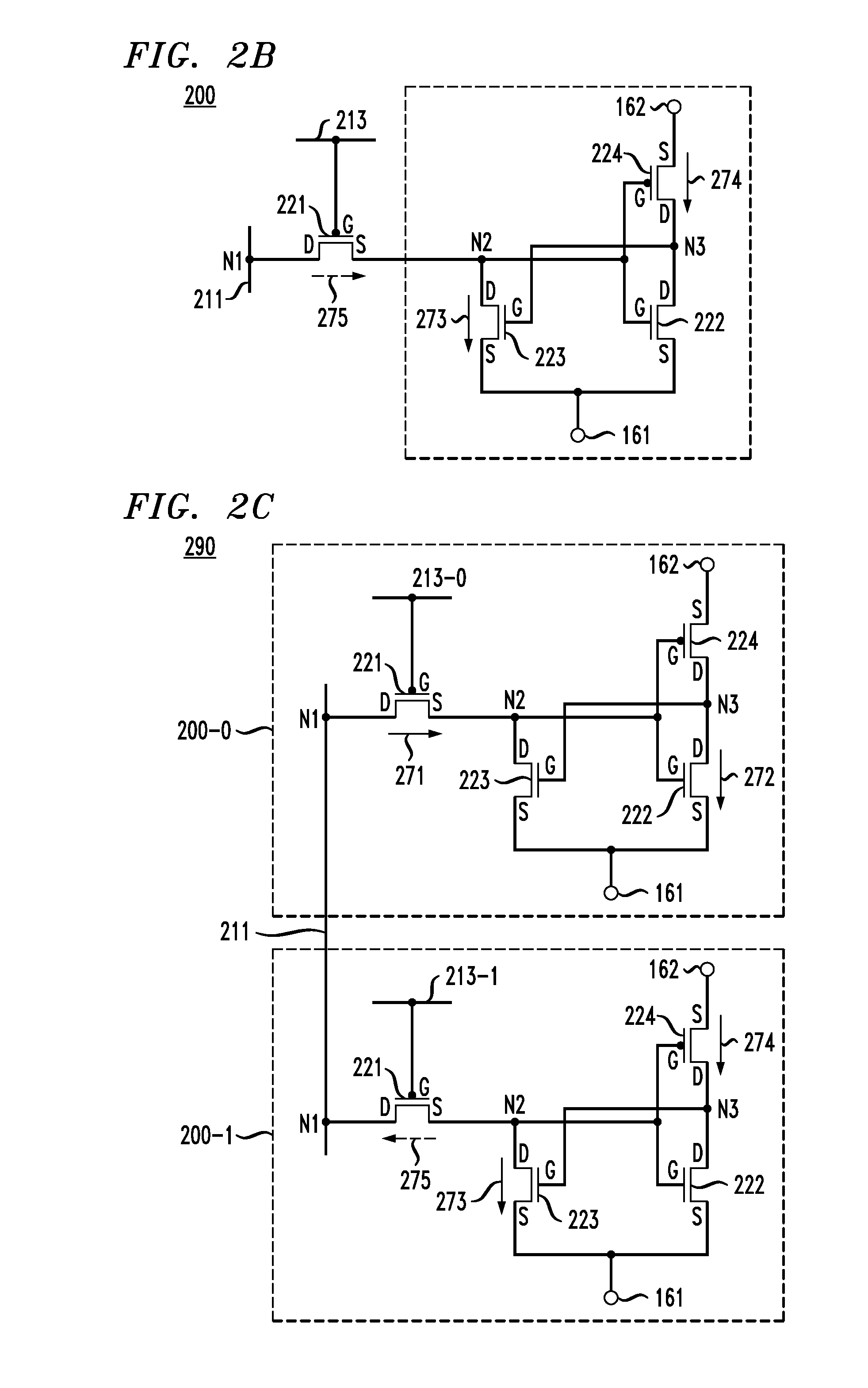
Aspects of the present invention will be described herein in the context of illustrative embodiments of a four-transistor (4T) SRAM cell adapted to utilize leakage current as a storage mechanism for reducing a size of the memory cell without significantly impacting performance of the cell. In accordance with other aspects of the invention, an exemplary memory circuit employing a plurality of memory cells and an illustrative method for forming a memory cell according to an embodiment of the invention are also described. It is to be appreciated, however, that the techniques of the present invention are not limited to the specific method and circuits shown and described herein. Rather, embodiments of the invention are directed broadly to techniques for beneficially utilizing leakage current in a memory cell in order to reduce a size of the cell without significantly impacting reliability or performance, or increasing overall current in the memory cell. For this reason, numerous modific...


PUM


Abstract

A memory cell comprises a storage element including a transistor and an inverter. The inverter has an input coupled to a first source/drain of the transistor at a first node and has an output coupled to a gate of the transistor at a second node. The transistor has a second source/drain coupled to a voltage supply of the memory circuit. The memory cell further includes a switching element coupled to the storage element at the first node and being operative to selectively access the storage element as a function of a control signal supplied to a control input of the switching element. The storage element is operative to store at least first and second data states. The first data state is retained in the storage element by maintaining the first node at a first voltage level by leakage current and by maintaining the second node at a second voltage level by active current. The second data state is retained in the storage element by maintaining the first node at the second voltage level and the second node at the first voltage level by respective active currents.

Description

FIELD OF THE INVENTIONThe present invention relates generally to the electrical, electronic, and computer arts, and more particularly relates to memory cells.BACKGROUND OF THE INVENTIONPower dissipation of an integrated circuit (IC) is composed of active power and leakage power. Leakage power is proportional to leakage current and, typically, serves no useful purpose in most conventional ICs. In recent IC fabrication technologies, leakage currents have increased and become a critical concern. A major source of leakage current is current flowing between the source and drain junctions of a field effect transistor (FET) when the FET is biased in an “off” state. An example is sub-threshold leakage current which flows between the source and drain when the FET is turned off.Embedded memory, which includes, for example, static random access memory (SRAM), is a major component in modern ICs. SRAM typically comprises many memory cells, for example, millions of memory cells. Leakage current m...

Claims


Application Information

Patent Timeline
Patent Type & Authority Applications(United States)
IPC IPC(8): G11C11/00G11C5/14
CPCG11C11/412
Inventor MCPARTLAND, RICHARD J.PHAM, HAI QUANGWERNER, WAYNE E.
Owner LSI CORPORATION
Why Eureka
Try Eureka