Semiconductor laser device, optical pickup device and semiconductor device

a laser device and semiconductor technology, applied in semiconductor lasers, semiconductor/solid-state device details, semiconductor laser structural details, etc., can solve the problems of deteriorating laser element reliability, inability to easily block or seal off the opening of the silicon substrate with a translucent sealing member, and inability to achieve the effect of reducing the shift or displacement of the optical axis occurring in the emitted laser and sealing a packag

Inactive Publication Date: 2011-06-30
SANYO ELECTRIC CO LTD
View PDF15 Cites 52 Cited by
  • Summary
  • Abstract
  • Description
  • Claims
  • Application Information

AI Technical Summary

Benefits of technology

[0128]Also, in the second embodiment, the semiconductor laser element 50 is directly bonded to the bottom face 216 of the recess 211, so that the irradiation range of the laser light irradiated to the inner wall surface 212 (metallic reflective film 270) can be further shifted toward the bottom face 216 side by as much as a degree to which the emission position of the laser light is further lowered (the direction C2). This structures allows the laser light having an elliptically-shaped pattern to be reliably irradiated to the inner wall surface 212 (metallic reflective film 270). In particular, when a semiconductor laser element that emits the laser light having a larger spread angle is to be used, the laser light can be reliably irradiated to the inner wall surface 212 (metallic reflective film 270) without the underside of the sealing glass 60 being directly irradiated with the upper edge of the laser light. Other advantageous effects achieved by the second embodiment are similar to those of the above-described first embodiment.
[0129]A third embodiment is now described with reference to FIG. 14 to FIG. 16. In a semiconductor laser device 300, according to the third embodiment, which differs from the semiconductor laser device 100 of the above-described first embodiment, a description is given of a case where a recess 311 in which the semiconductor laser element 50 is placed is provided such that a photo solder resist 350, or an insulator, blocks an opening 301b (see FIG. 16) in one side (C2 side) of a Si(100) substrate 310 having through-holes 301. FIG. 15 is a cross-sectional view taken along line 3000-3000 of FIG. 14. Each component identical to that of the first embodiment is given the identical reference numeral in FIG. 14. Note that the Si(100) substrate 310 is an example of “semiconductor substrate” in claim phraseology (WHAT IS CLAIMED), whereas the photo solder resist 350 is an example of “support base” in claim phraseology. Also, the opening 301b is an example of “second opening” in claim phraseology.
[0130]As shown in FIG. 15, the semiconductor laser device 300 according to the third embodiment of the present invention includes (1) a Si(100) substrate 310, having a high resistivity (insulation properties), in which a through-hole 301 penetrates in a thickness direction (direction C), (2) a photo solder resist 350 for forming the recess 311 by blocking an opening 301b (see FIG. 16) at the lower side (C2 side) of the through-hole 301 in such a manner that the photo solder resist 350 is bonded to an underside 310b of the Si(100) substrate 310 via an adhesive resin 351, (3) a semiconductor laser element 50 placed on a bottom face 316 of the recess 311 via a submount 30, and (4) a translucent sealing glass 60 for blocking an opening 311a at an upper side (C2 side) of the recess 311 wherein the sealing glass 60 is mounted on a top face 310a of the Si(100) substrate 310. Here, the photo solder resist is an insulating film using a photosensitive resin, by which an exposed part only is structurally altered so as not to be dissolved by a solvent and the like. Note that the opening 311a is an example of “first opening” in claim phraseology.
[0131]According to the third embodiment, in a fabrication process described later, anisotropic etching is, as shown in FIG. 15, performed on the Si(100) substrate 310 having a main surface (top face 310a) tilted about 9.7 degrees relative to an approximately (100) plane, thereby forming the four inner wall surfaces 312, 313, 314 and 315 (composed of Si(111) planes) in the Si(100) substrate 310. The use of the Si(100) substrate 310 having the main surface tilted about 9.7 degrees allows the formation of the inner wall surface 312 which is tilted at an inclination angle α of about 45 degrees relative to a top face 350a of the photo solder resist 350 (relative to the bottom face 316). At the same time, the use of the Si(100) substrate 310 allows the formation of the inner wall surface 313 which is tilted at an inclination angle β of about 64.4 degrees relative to the top face 350a (bottom face 316). The inner wall surfaces 314 and 315 (see FIG. 14) are each formed such that each of them is tilted at an inclination angle γ of about 54.7 degrees relative to the top face 350a (bottom face 316). The inner wall surfaces 312 to 315 are an example of “inner wall surface” in claim phraseology. The inner wall surface 312 is an example of “first region of an inner wall surface” and “first tilted surface” in the claim phraseology, whereas the inner wall surface 313 is an example of “second region of an inner wall surface” and “second tilted surface” in the claim phraseology.
[0132]In the third embodiment, the four inner wall surfaces 312, 313, 314 and 315 and the adhesive resin 351 formed on top (the surface on a C1 side) of the photo solder resist 350 constitute the recess 311. The adhesive resin 351 is used to join the Si(100) substrate 310 and the photo solder resist 350 together. As shown in FIG. 15, the bottom face 316 of the recess 311 is constituted substantially of a part of the upper face of the adhesive resin 351. The Si(100) substrate 310 has a thickness of about 500 μm; i.e., the distance between the top face 310a and the underside 310b of the Si(100) substrate 310 is about 500 μm.
[0133]In the third embodiment, a wiring electrode 331, made of Cu or the like, which is used to die-bond the submount 30 is formed in a region (a region constituting the bottom face 316 of the recess 311) exposed inside the recess 311, wherein said region exposed inside the recess 311 is a part of the upper face of the photo solder resist 350 (adhesive resin 351). With such an arrangement described as above, the back side (C2-side surface) of the submount 30 is bonded, in a position closer to an A1 side (inner wall surface 312 side) from an approximate center in the recess 311, to the surface of the wiring electrode 331 via an electrically conductive adhesion layer (not shown). In other words, the submount 30 to which the semiconductor laser element 50 is bonded is placed on top of a “support base”, in the claim phraseology, which is constituted by the photo solder resist 350 and the wiring electrode 331 formed on the solder resist 350. The wiring electrode 331 exposed inside the recess 311 has a plane area larger than that of the submount 30, and the submount 30 is placed within a region where the wiring electrode 331 is formed. The wiring electrode 331 has a leader wiring portion 331a that extends from, a position in which the submount 30 is placed, along the direction A1. The surface of the wiring electrode 331 exposed on the bottom surface 316 is an example of “bottom face” in the claim phraseology.

Problems solved by technology

Further, the reliability of the laser element deteriorates, thereby creating an undesired situation.
This causes a problem that the opening of the recess of the silicon substrate cannot be easily blocked by or sealed off with a translucent sealing member.
In other words, the inconvenience is caused by the installation errors of the semiconductor element relative to the package, the transparent substrate relative to the package, and the mirror relative to the transparent substrate, respectively.
As a result, a problem arises that a large shift or displacement in the optical axis occurs in the laser light emitted after the reflection by the mirror due to the above-described respective install errors.

Method used


Image

  • Semiconductor laser device, optical pickup device and semiconductor device
  • Semiconductor laser device, optical pickup device and semiconductor device
  • Semiconductor laser device, optical pickup device and semiconductor device

Examples


first embodiment

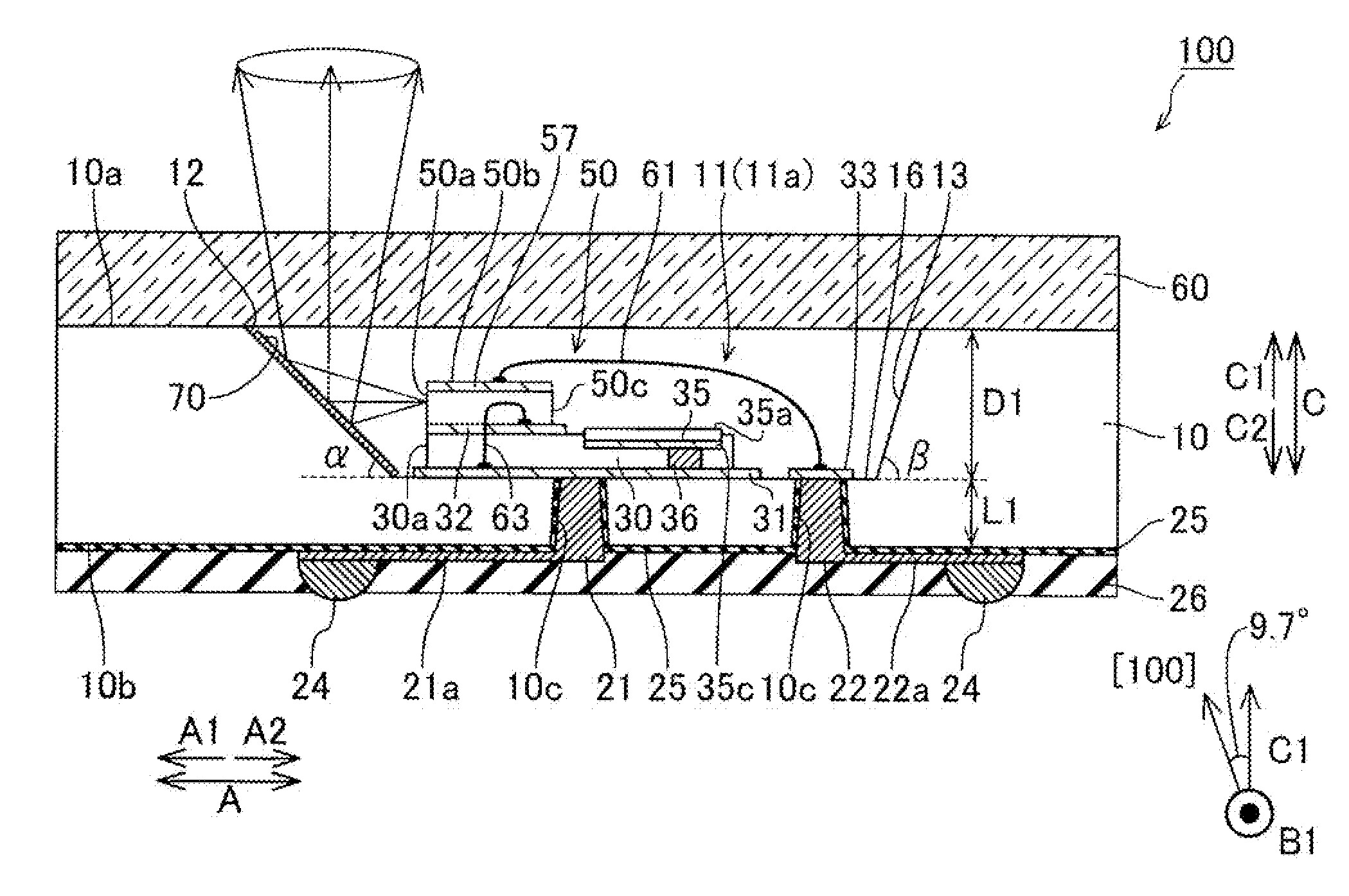
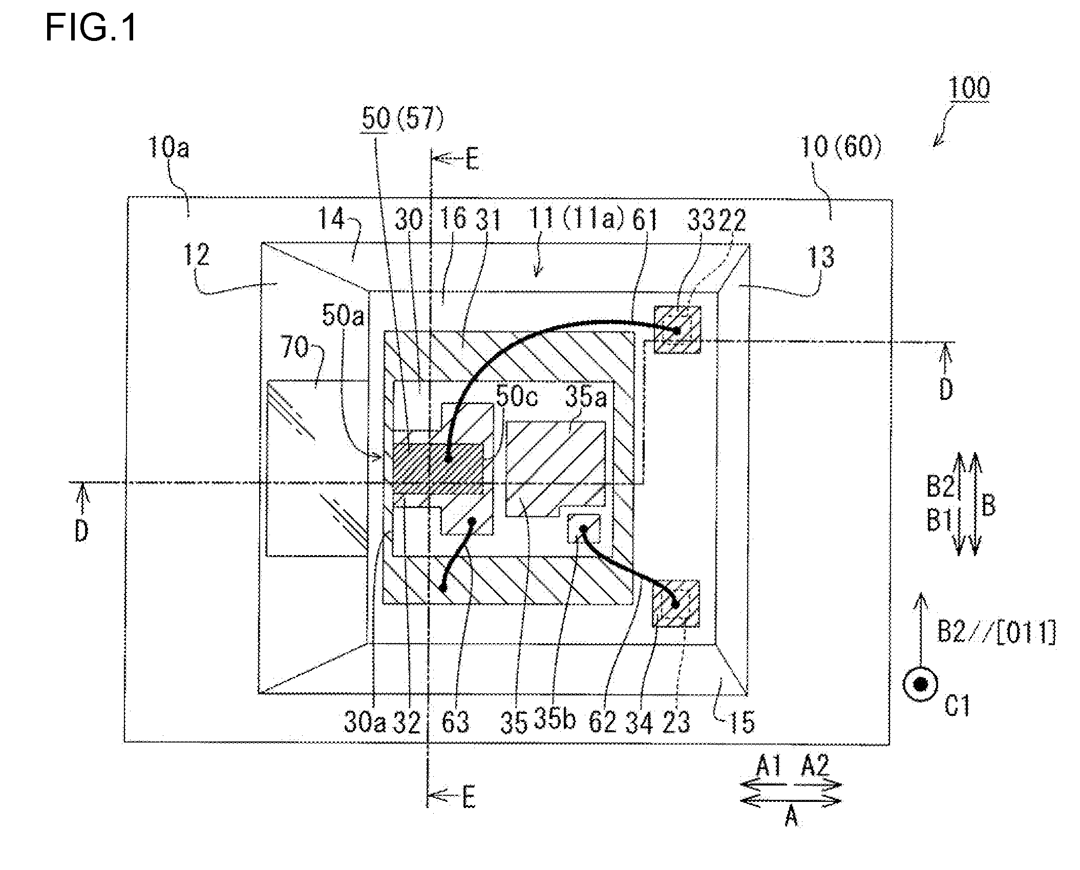
[0075]Referring to FIG. 1 to FIG. 4, a description is first given of a semiconductor laser device 100 according to a first embodiment of the present invention. FIG. 2 is a cross-sectional view of FIG. 1 taken along line D-D, and FIG. 4 is a cross-sectional view of FIG. 1 taken along line E-E.

[0076]As shown in FIG. 2, the semiconductor laser device 100 according to the first embodiment of the present invention includes (1) a Si(100) substrate 10, having a high resistivity, in which a recess 11 dent from above (C1 side) toward below (C2 side) is formed, (2) a semiconductor laser element 50 placed on a bottom face 16 of the recess 11 via a submount (base) 30, and (3) a translucent sealing glass 60 for blocking an opening 11a of the recess 11 wherein the sealing glass 60 is mounted on a top face 10a of the Si(100) substrate 10. Note that the Si(100) substrate 10 is an example of “semiconductor substrate” in claim phraseology (WHAT IS CLAIMED), whereas the opening 11a is an example of “f...

second embodiment

[0116]A second embodiment is now described with reference to FIG. 2 and FIG. 11 to FIG. 13. In a semiconductor laser device 200, according to the second embodiment, which differs from the semiconductor laser device 100 of the above-described first embodiment, a description is given of a case where the back side of the semiconductor laser element 50 is directly fixed onto the surface region of a bottom face 216 of a recess 211. FIG. 12 is a cross-sectional view taken along line 2000-2000 of FIG. 11. Each component identical to that of the first embodiment is given the identical reference numeral in Figures.

[0117]As shown in FIG. 11, the semiconductor laser device 200 according to the second embodiment of the present invention includes (1) a Si(100) substrate 210, having a high resistivity, in which a recess 211 dent from above (C1 side) toward below (C2 side) is formed, (2) a semiconductor laser element 50 bonded to a surface of a bottom face 216 of the recess 211, and (3) a transluc...

third embodiment

[0129]A third embodiment is now described with reference to FIG. 14 to FIG. 16. In a semiconductor laser device 300, according to the third embodiment, which differs from the semiconductor laser device 100 of the above-described first embodiment, a description is given of a case where a recess 311 in which the semiconductor laser element 50 is placed is provided such that a photo solder resist 350, or an insulator, blocks an opening 301b (see FIG. 16) in one side (C2 side) of a Si(100) substrate 310 having through-holes 301. FIG. 15 is a cross-sectional view taken along line 3000-3000 of FIG. 14. Each component identical to that of the first embodiment is given the identical reference numeral in FIG. 14. Note that the Si(100) substrate 310 is an example of “semiconductor substrate” in claim phraseology (WHAT IS CLAIMED), whereas the photo solder resist 350 is an example of “support base” in claim phraseology. Also, the opening 301b is an example of “second opening” in claim phraseol...


PUM


Abstract

A semiconductor laser device includes a Si(100) substrate in which a recess having an opening and a bottom face surrounded by inner wall surfaces is formed, a semiconductor laser element placed on the bottom face, and a translucent sealing glass, mounted on top of the Si(100) substrate, which seals the opening. The laser light emitted from the semiconductor laser element is reflected by a metallic reflective film formed on the inner wall surface and then transmits through the sealing glass so as to be emitted externally.

Description

[0001]This application is based upon and claims the benefit of priority from the prior Japanese Patent Applications No. 2009-298415, filed on Dec. 28, 2009 and Japanese Patent Application No. 2010-083911, filed on Mar. 31, 2010, the entire contents of which are incorporated herein by reference.BACKGROUND OF THE INVENTION[0002]1. Field of the Invention[0003]The present invention relates to a semiconductor laser device and an optical pickup device, and it particularly relates to a semiconductor laser device and an optical pickup device both employing a semiconductor laser element.[0004]2. Description of the Related Art[0005]The semiconductor laser element is conventionally in widespread use as a light source of an optical disk system, an optical communication system and the like. In particular, a semiconductor laser element emitting a laser light in the visible light band of about 380 nm to about 780 nm is in practical use as the light source for the recording and playback / reproductio...

Claims


Application Information

Patent Timeline
Patent Type & Authority Applications(United States)
IPC IPC(8): H01S5/02
CPCB82Y20/00H01S5/02208H01L2924/1461H01L2224/45144H01L2224/49175H01L2224/48091H01L24/97H01S5/0222H01S5/0224H01S5/02248H01S5/02276H01S5/02292H01S5/0683H01S5/34333H01S5/4031H01S5/4087H01L2924/00014H01L2924/00H01L2224/73265H01L2924/12043H01L2924/15788H01L2924/16195H01S5/02255H01S5/02325H01S5/0234H01S5/02345
Inventor OKAYAMA, YOSHIOINOUE, YASUNORIGOTO, TAKENORIMORI, KAZUSHIOTA, YUUKIMATSUBARA, NAOTERU
Owner SANYO ELECTRIC CO LTD
Why Eureka
Try Eureka