Ld-driver improving falling edge of driving signal

a technology of driver and driving signal, applied in semiconductor lasers, laser details, instruments, etc., can solve the problems of increasing power consumption, complex layout of two emitter followers, and increasing power consumption

Inactive Publication Date: 2011-07-07
SUMITOMO ELECTRIC IND LTD
View PDF3 Cites 16 Cited by
  • Summary
  • Abstract
  • Description
  • Claims
  • Application Information

AI Technical Summary

Benefits of technology

[0011]An aspect of the present invention is, in an LD driver circuit including a push-pull driver for driving the output transistor, to reduce a time lag between the push driver and the pull driver as suppressing the increase of the power consumption of the push-pull driver. The LD driver according to the present invention comprises an inverting amplifier, an emitter follower, a current-mirror circuit, and an output transistor. The inverting amplifier receives an input signal and outputs an amplified signal. The emitter follower includes a buffer transistor and a current source connected in series to the buffer transistor. The buffer transistor with the emitter follower connection receives the amplified signal and outputs a driving signal in the emitter thereof. The output transistor receives the driving signal and drives the LD. The current-mirror circuit, which is connected in series to the inverting amplifier, reflects a current flowing in the inverting amplifier to a mirror current that pulls out carriers accumulated in the input capacitance of the output transistor. The buffer transistor in the emitter follower and a mirror transistor that provides the mirror current constitute the push-pull circuit for driving the output transistor.
[0013]While, setting the input signal in HIGH level, the amplified signal turns LOW level to flow a current therein, but the current-mirror circuit connected in series to the inverting amplifier may reflect the current flowing in the inverting amplifier to the mirror transistor. The charges accumulated in the input capacitor of the output circuit may be discharged by this mirror current, which accelerates the falling edge of the driving signal. Thus, the LD driver according to the present invention may accelerate the falling edge of the driving signal, namely, the driving signal of the output circuit, without increasing the current determined by the current source in the emitter follower. The mirror current may be generated only for a period when the input signal stays in HIGH level, which may suppress the increase of the power consumption.
[0014]The LD driver of the present invention may reduce the time lag between the signal path from the input to the input of the output circuit through the emitter follower and another path through the current-mirror circuit; because the former path includes two transistors, one is in the inverting amplifier and the other is in the emitter follower, while, the latter path includes also two transistors, one is in the inverting amplifier and the other is in the current mirror. Thus, the LD driver of the invention may suppress the time lag between the push driver and the pull driver, which simplifies the circuit layout.
[0016]In an modification of the LD driver according to the present invention, the mirror transistor may be driven by a spiked signal synchronized with one of the amplified signal and the driving signal, both of which have the same phase. The mirror transistor driven by the spiked signal may generate a spiked current synchronized with the falling edge of the driving signal. The spiked current may further accelerate the discharging of the carriers accumulated in the input capacitor Cbe of the output circuit. In this modification, the mirror ratio of the current-mirror circuit may be less than unity, which means that a lesser mirror current flows in a stable state and a spiked large current may be provided only at the falling edge of the driving signal.

Problems solved by technology

However, further reduction of the impedance requires the increase of the current, 113 and 114, flowing in the emitter follower, which results in the increase of the power consumption.
Thus, in the LD driver 100B shown in FIG. 12, the power consumption thereof increases and the layout connecting two emitter followers becomes complex.

Method used


Image

  • Ld-driver improving falling edge of driving signal
  • Ld-driver improving falling edge of driving signal
  • Ld-driver improving falling edge of driving signal

Examples


Embodiment Construction

[0030]Next, some preferred embodiments of an LD driver according to the present invention will be described as referring to accompanying drawings. In the description of the drawings, the same or like numerals or the symbols will refer to the same or like elements without overlapping explanations. Although the specification concentrates on bipolar transistors with a base as the control electrode, and an emitter and a collector as the current electrode, the active devices used in the circuit may be the FET with a gate as the control electrode, and a drain and a source as the current electrode.

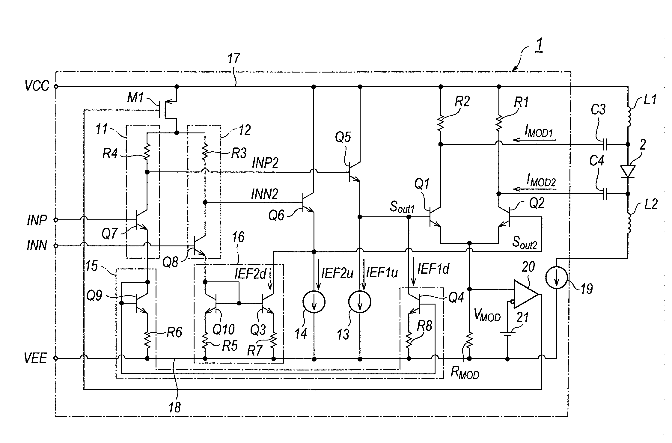
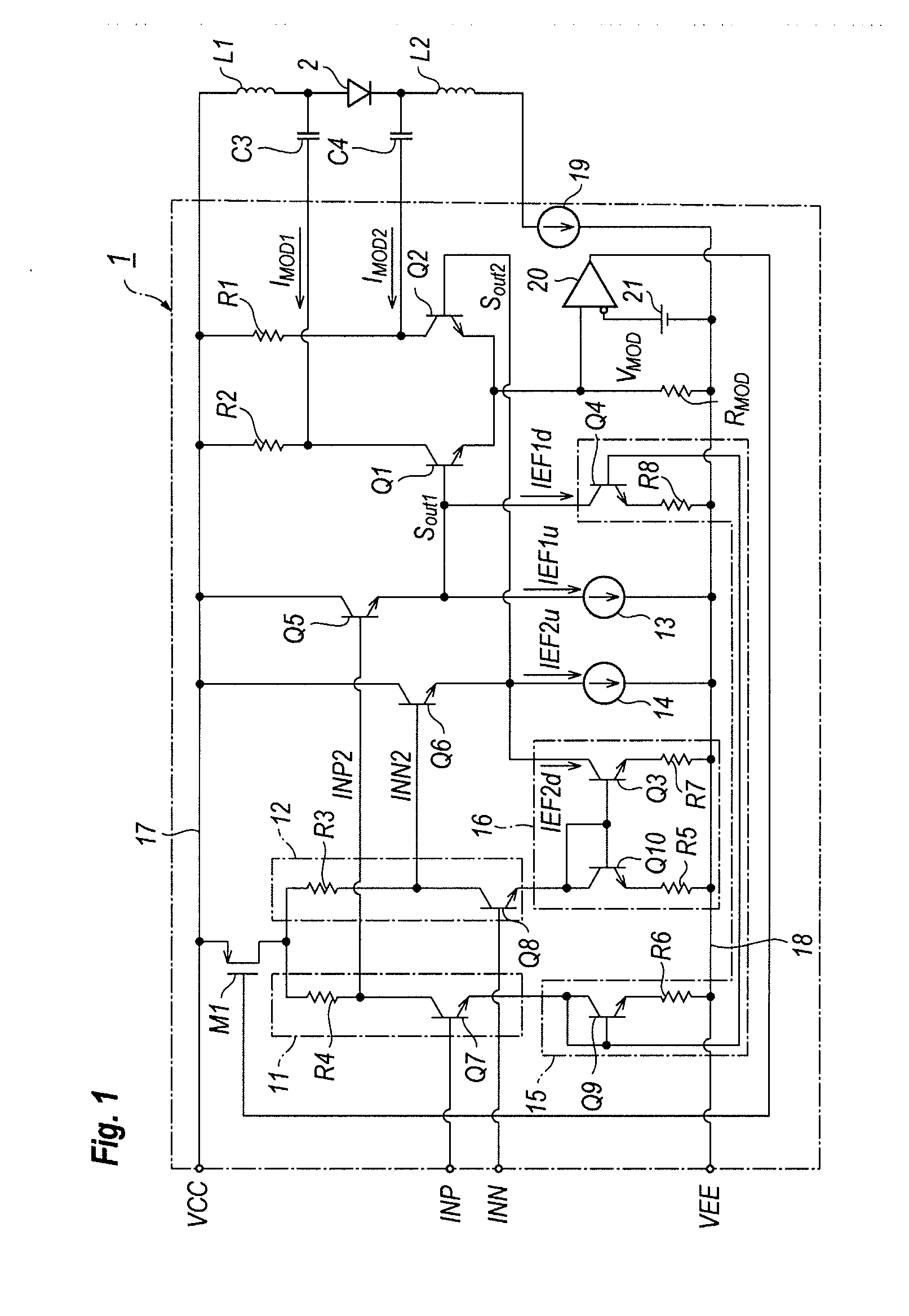
[0031]FIG. 1 is a circuit diagram of an LD-Driver according to an embodiment of the present invention. The LD-Driver 1 generates a differential current, IMOD1 and IMOD2 to drive the LD 2. The LD driver 1 comprises the first and second control units.

[0032]The first control unit provides the driving signal SOUT1 to the transistor Q1 in the output circuit by receiving the input signal INP with a pos...


PUM


Abstract

An LD driver is disclosed, which improves the rising and falling times of the driving current for the LD. The LD driver includes an inverting amplifier, an emitter follower connected in down stream of the inverting amplifier, a driving transistor driven by the emitter follower, and a current-mirror circuit connected in series to the inverting amplifier. The mirror current generated from the current flowing in the inverting amplifier is provided to the output of the emitter follower served for discharging the input capacitance of the driving transistor.

Description

BACKGROUND OF THE INVENTION[0001]1. Field of the Invention[0002]The present invention relates to a high-speed driver circuit for a semiconductor laser diode (hereinafter denoted as LD), in particular.[0003]2. Related Background Art[0004]FIG. 11 shows a convention LD driver circuit disclosed in the U.S. Pat. No. 7,145,928. The LD driver 100A shown in FIG. 11, which summarizes primary portions of the circuit disclosed therein, comprises a bias current source including a series circuit of an inductor 102 and a current source 103; and a modulation current source including a paired transistor, 104 and 105, with another current source 106. One of the paired transistors 104 is connected to the LD 101, while, the other 105 is connected to a dummy resistor 107. Respective emitters of the paired transistor are commonly connected to the current source 106.[0005]The paired transistor, 104 and 105, receives a driving signal, which may be a differential signal, from the emitter followers. Each of...

Claims


Application Information

Patent Timeline
Patent Type & Authority Applications(United States)
IPC IPC(8): H01S3/00G05F5/00
CPCH01S5/0428
Inventor TANAKA, KEIJI
Owner SUMITOMO ELECTRIC IND LTD
Why Eureka
Try Eureka