Microstructure manufacturing method

a manufacturing method and microstructure technology, applied in the direction of material analysis using wave/particle radiation, instruments, radiofrequency control devices, etc., to achieve the effects of high degree of precision, high aspect ratio, and easy manufacturing

Active Publication Date: 2011-07-14
CANON KK
View PDF10 Cites 17 Cited by
  • Summary
  • Abstract
  • Description
  • Claims
  • Application Information

AI Technical Summary

Benefits of technology

[0008]The present invention is directed to a microstructure manufacturing method enabling easy ma

Problems solved by technology

However, Japanese Patent Application Laid-Open No. 2007-203066 does not dis

Method used


Image

  • Microstructure manufacturing method
  • Microstructure manufacturing method
  • Microstructure manufacturing method

Examples


Embodiment Construction

[0019]Various exemplary embodiments, features, and aspects of the invention will be described in detail below with reference to the drawings.

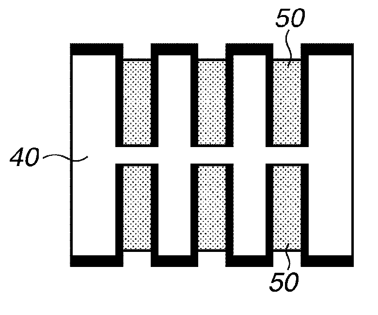
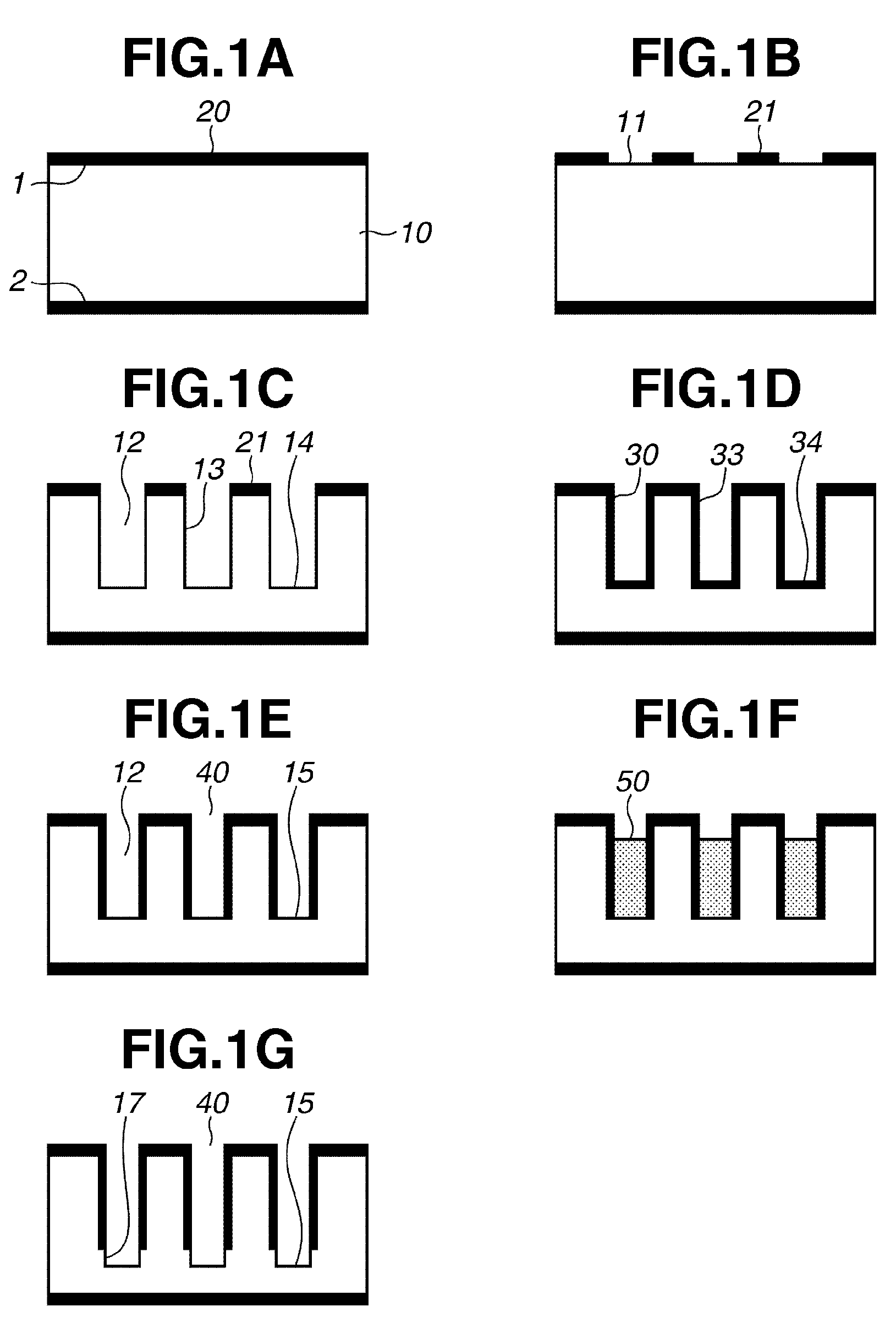
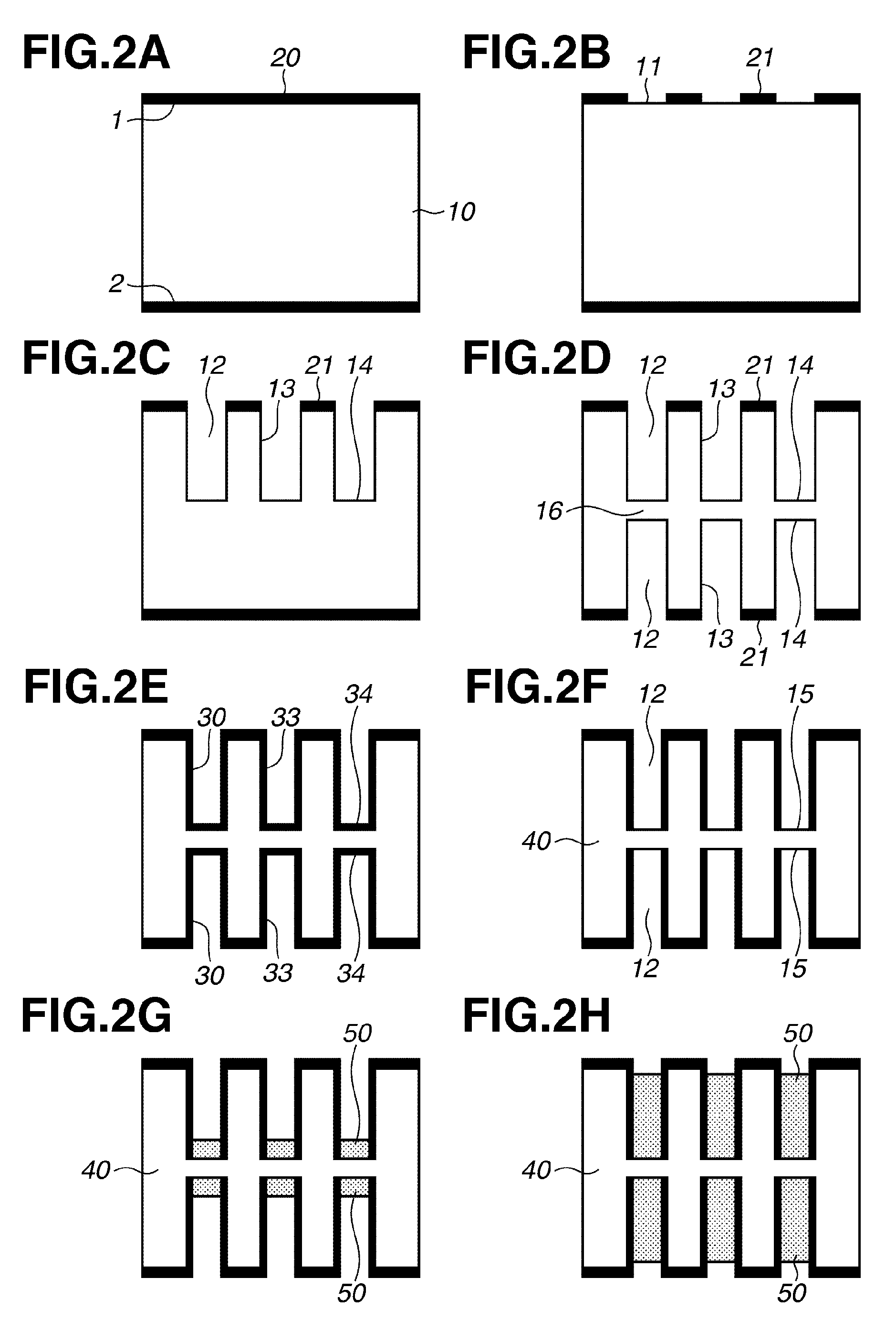
[0020]FIG. 1 illustrates a first exemplary embodiment of the microstructure manufacturing method according to the present invention. This manufacturing method is a method including forming a microstructure on one surface of an Si substrate, and forming a metal microstructure by applying electrolytic plating to the inside of the Si microstructure while using the Si microstructure as a mold.

[0021]First, a first insulating film is formed on the front surface and the back surface of the Si substrate (first process). As illustrated in FIG. 1A, the first insulating film 20 is formed on a front surface 1 and a back surface 2 of an Si substrate 10. The size and thickness of the Si substrate 10 can be determined according to a desired microstructure. Further, the resistivity of the Si substrate 10 is 10 Ωcm or less, preferably or optimally 0.1 Ωcm or le...


PUM


Abstract

A microstructure manufacturing method includes forming a first insulating film on an Si substrate, exposing an Si surface by removing a part of the first insulating film, forming a recessed portion by etching the Si substrate from the exposed Si surface, forming a second insulating film on a sidewall and a bottom of the recessed portion, forming an Si exposed surface by removing at least a part of the second insulating film formed on the bottom of the recessed portion, and filling the recessed portion with a metal from the Si exposed surface by electrolytic plating.

Description

BACKGROUND OF THE INVENTION[0001]1. Field of the Invention[0002]The present invention relates to a method for manufacturing a microstructure, and, in particular, to a method for manufacturing a microstructure by electrolytic plating of a metal with use of a mold, especially a microstructure having a high aspect ratio.[0003]2. Description of the Related Art[0004]A micro fine structure having periodic structure, especially a high aspect ratio structure is needed in a large number of fields. For example, the X-ray absorption characteristic of a microstructure composed of gold is utilized in a nondestructive test of an object as an industrial application, and also utilized in, for example, radiography as a medical application. A microstructure in these applications forms a contrast image by utilizing an absorption difference in X-ray transmission depending on constituent elements and a density variation in an object or a biological object, and is called the X-ray absorption contrast met...

Claims


Application Information

Patent Timeline
IPC IPC(8): G01T1/24H01L21/3205H01L29/06
CPCB81C1/00619H01L21/32051H01L21/31111G01T1/295G01N23/20075G21K1/06
Inventor WANG, SHINANNAKAMURA, TAKASHITESHIMA, TAKAYUKISETOMOTO, YUTAKAWATANABE, SHINICHIRO
Owner CANON KK
Why Eureka
Try Eureka