Back-gated fully depleted soi transistor

Inactive Publication Date: 2011-07-14
GLOBALFOUNDRIES INC
View PDF14 Cites 216 Cited by
  • Summary
  • Abstract
  • Description
  • Claims
  • Application Information

AI Technical Summary

Benefits of technology

[0008]According to an embodiment of the present invention, a fully depleted semiconductor-on-insulator (FDSOI) transistor structure includes a back gate electrode having a limited thickness and aligned to a front gate electrode. The back gate electrode is formed in a first substrate by ion implantation of dopants through a first oxide cap layer, which functions as a screening oxide layer to limit the depth of ion implantation and to prevent channeling of ion

Problems solved by technology

However, detrimental short-channel effects can lead to high off-state leakage currents in CMOS devices, thereby increasing the power consumption.
In case of extreme short-channel effects, CMOS circuits fail to operate.
The overlap of the back gate electrode with the source/drain region leads to increased parasitic capacitance, which leads to slower FET switching speed.
High energy implants through the thin SOI re

Method used


Image

  • Back-gated fully depleted soi transistor
  • Back-gated fully depleted soi transistor
  • Back-gated fully depleted soi transistor

Examples


first embodiment

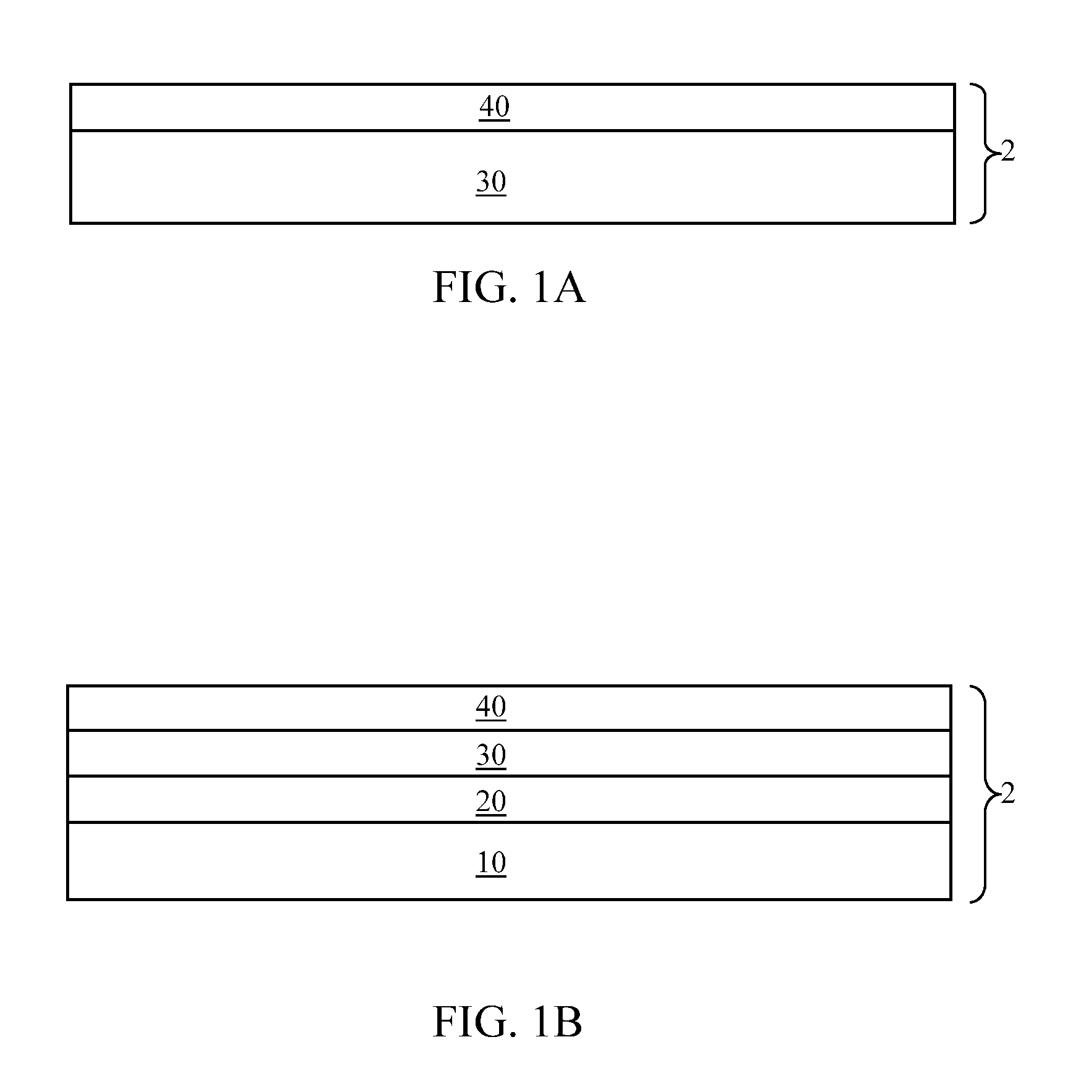
[0048]Referring to FIG. 5A, the second handle substrate 110 can have the same composition and the same thickness as the first handle substrate 10. The second buried insulator layer 120 can have the same composition and the same thickness as the first buried insulator layer 20. The second semiconductor layer 130 can have the same composition as the first semiconductor layer 30. Typically, the semiconductor material of the second semiconductor layer 130 comprises silicon. Preferably, the second semiconductor layer 130 is single crystalline. The thickness of the second semiconductor layer 130 can be from 20 nm to 300 nm, although lesser and greater thicknesses can also be employed. The composition and the thickness of the second oxide cap layer 140 can be the same as in the

[0049]Hydrogen ions are implanted through the second oxide cap layer 140 into the second semiconductor layer 130 to form an embedded layer of hydrogen atoms therein in the same manner as in the first embodiment. Afte...

third embodiment

[0060]Referring to FIG. 7B, the second substrate 4 is flipped upside down over a second exemplary structure for the first substrate 2. The second exemplary structure is the same as in the The second substrate 4 and the first substrate 2 are brought to physical contact with each other. The top surface of the first oxide cap layer 40 contacts the top surface (which is now located at the bottom of the second substrate 4) of the second oxide cap layer 140.

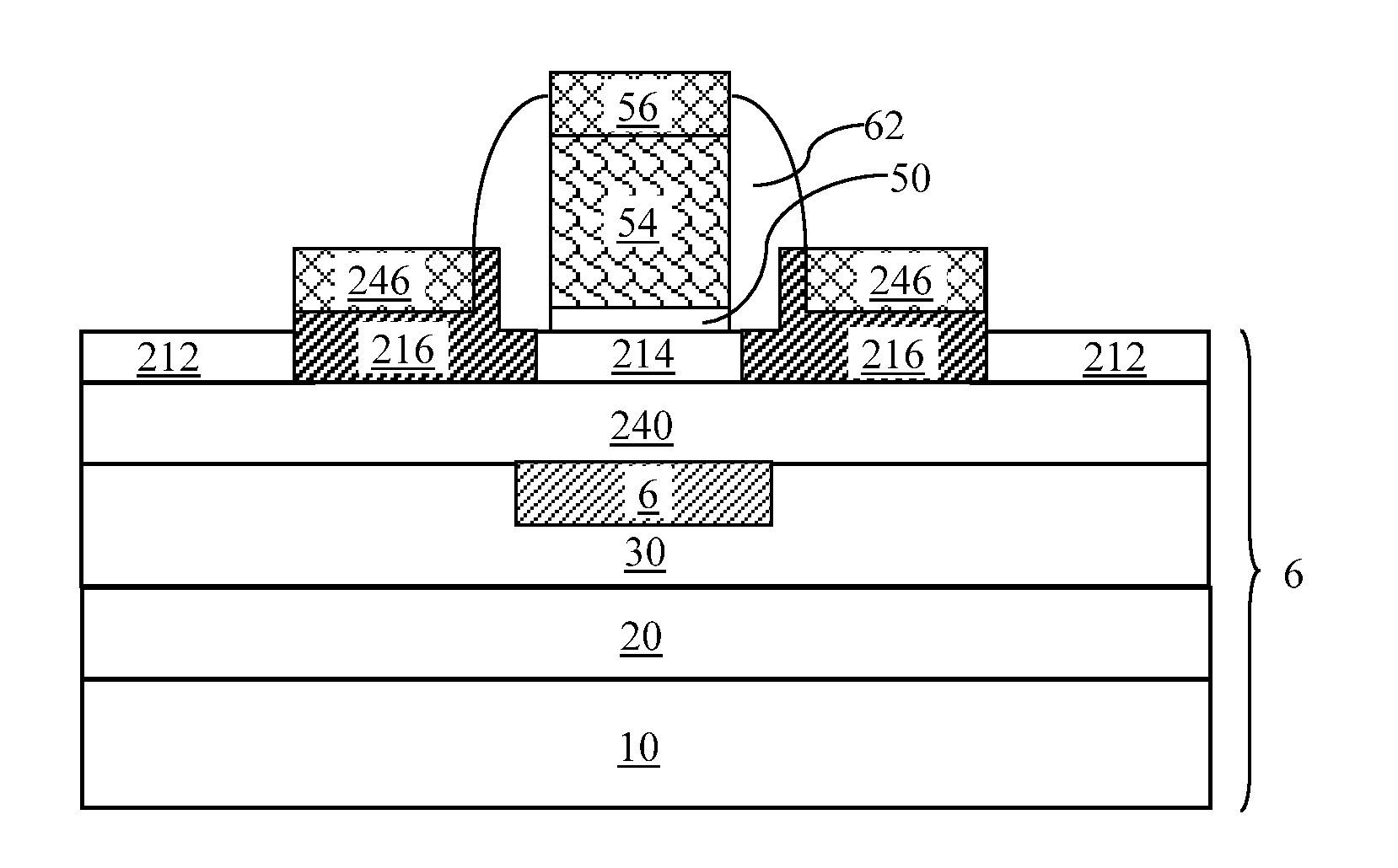
[0061]Referring to FIG. 7C, the first oxide cap layer 40 and the second oxide cap layer 140 are bonded by methods known in the art to form a buried oxide layer 240. The first substrate 2 and the second substrate 4 collectively form a bonded substrate 6 upon bonding. The thickness of the buried oxide layer 240 can be from 2 nm to 50 nm, and preferably from 2 nm to 20 nm, although lesser and greater thicknesses can also be employed.

[0062]Referring to FIG. 7D, the assembly of the second handle substrate 110, the second buried insulator l...


PUM


Abstract

A fully depleted semiconductor-on-insulator (FDSOI) transistor structure includes a back gate electrode having a limited thickness and aligned to a front gate electrode. The back gate electrode is formed in a first substrate by ion implantation of dopants through a first oxide cap layer. Global alignment markers are formed in the first substrate to enable alignment of the front gate electrode to the back gate electrode. The global alignment markers enable preparation of a virtually flat substrate on the first substrate so that the first substrate can be bonded to a second substrate in a reliable manner.

Description

BACKGROUND[0001]The present invention relates to field-effect transistors (FETs), and more particularly to thin-body fully-depleted semiconductor-on-insulator (SOI) FETs including a back gate self-aligned to a front gate, and methods of manufacturing the same.[0002]Complementary metal-oxide semiconductor (CMOS) field-effect transistors (FETs) are employed in almost every electronic circuit application, such as signal processing, computing, and wireless communications. Scaling down the gate length of both N-channel FETs (NFETs) and P-channel FETs (PFETs) in CMOS circuits to shorter dimensions can increase the speed of the CMOS circuits. However, detrimental short-channel effects can lead to high off-state leakage currents in CMOS devices, thereby increasing the power consumption. In case of extreme short-channel effects, CMOS circuits fail to operate.[0003]Fully-depleted semiconductor-on-insulator (FDSOI) FETs with thin SOI bodies provide improved electrostatic integrity than thick-b...

Claims


Application Information

Patent Timeline
IPC IPC(8): H01L21/336
CPCG03F9/7084H01L2924/01019H01L21/6835H01L23/544H01L29/78648H01L2221/68318H01L2221/68363H01L2221/68377H01L2223/54426H01L2224/80006H01L2224/8013H01L2224/802H01L2924/12044H01L2924/13091H01L21/2652H01L21/2658H01L21/2654H01L21/26553H01L21/26506
Inventor CHANG, LELANDJI, BRIAN L.KUMAR, ARVINDMAJUMDAR, AMLANSAENGER, KATHERINESHI, LEATHENYAU, JENG-BANG
Owner GLOBALFOUNDRIES INC
Why Eureka
Try Eureka