
Floating grid module design for thin film silicon solar cells

a solar cell and floating grid technology, applied in the field of solar cells, can solve the problems of increasing the average solar cell cost, increasing the cell width, and increasing the overall performance of the average solar cell, and achieve the effect of enhancing the current conduction of the tco layer

Inactive Publication Date: 2011-07-28
APPLIED MATERIALS INC
View PDF6 Cites 19 Cited by
  • Summary
  • Abstract
  • Description
  • Claims
  • Application Information

AI Technical Summary

Benefits of technology

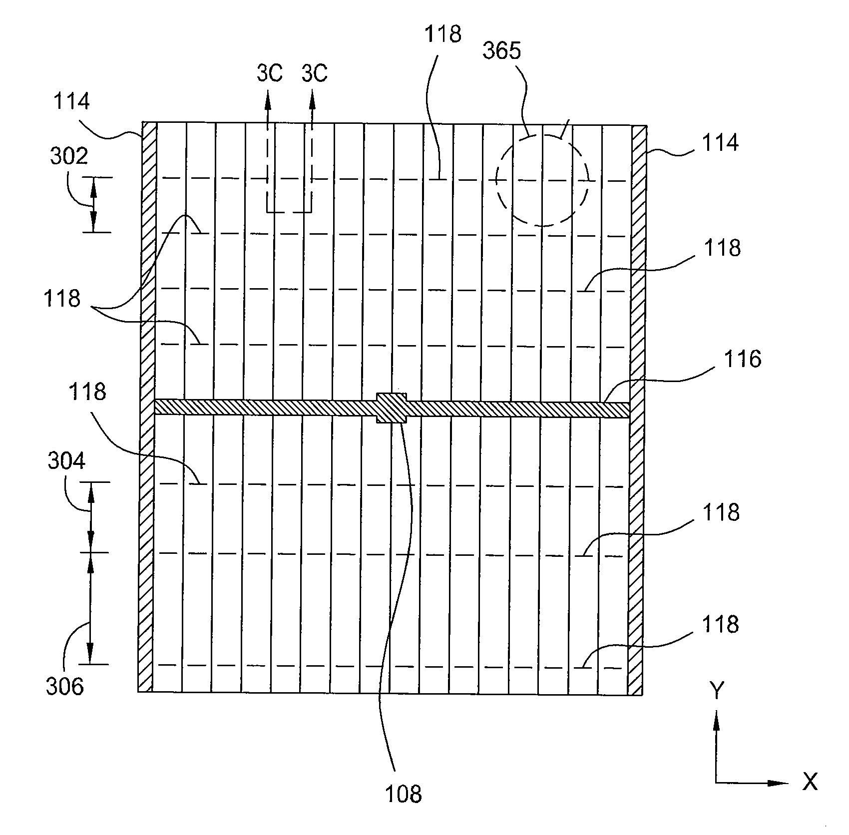
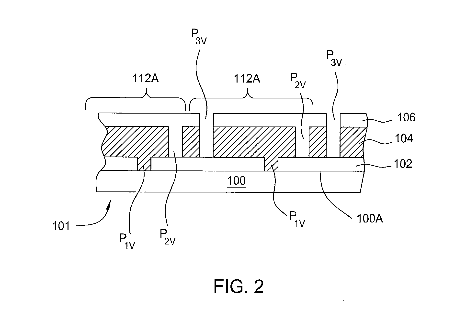
[0011]Embodiments of the present invention also provide a method for fabricating a series of solar cell array on a substrate, comprising providing a substrate having a TCO layer formed thereon, forming at least two vertical scribing lines in the TCO layer to isolate the TCO layer into individual cells, providing a plurality of electrical conductive paths electrically in contact within the TCO layer to enhance current conduction of the TCO layer, wherein the plurality of electrical conductive paths are substantially perpendicular to the plurality of scribing lines, and forming a silicon-containing film stack over the TCO layer.

Problems solved by technology

Usually, a single sheet solar cell alone does not have a sufficient output voltage for a PV module.
However, operators working under such a high power output will require a special protection and therefore, increases the average solar cell cost.
However, an increased cell width will also decrease overall performance since the series resistance from the front TCO layer is increased accordingly.
Meanwhile, wider cell widths also result in severe electrical losses in contact layers due to increasing cell current.

Method used


Image

  • Floating grid module design for thin film silicon solar cells
  • Floating grid module design for thin film silicon solar cells
  • Floating grid module design for thin film silicon solar cells

Examples


Embodiment Construction

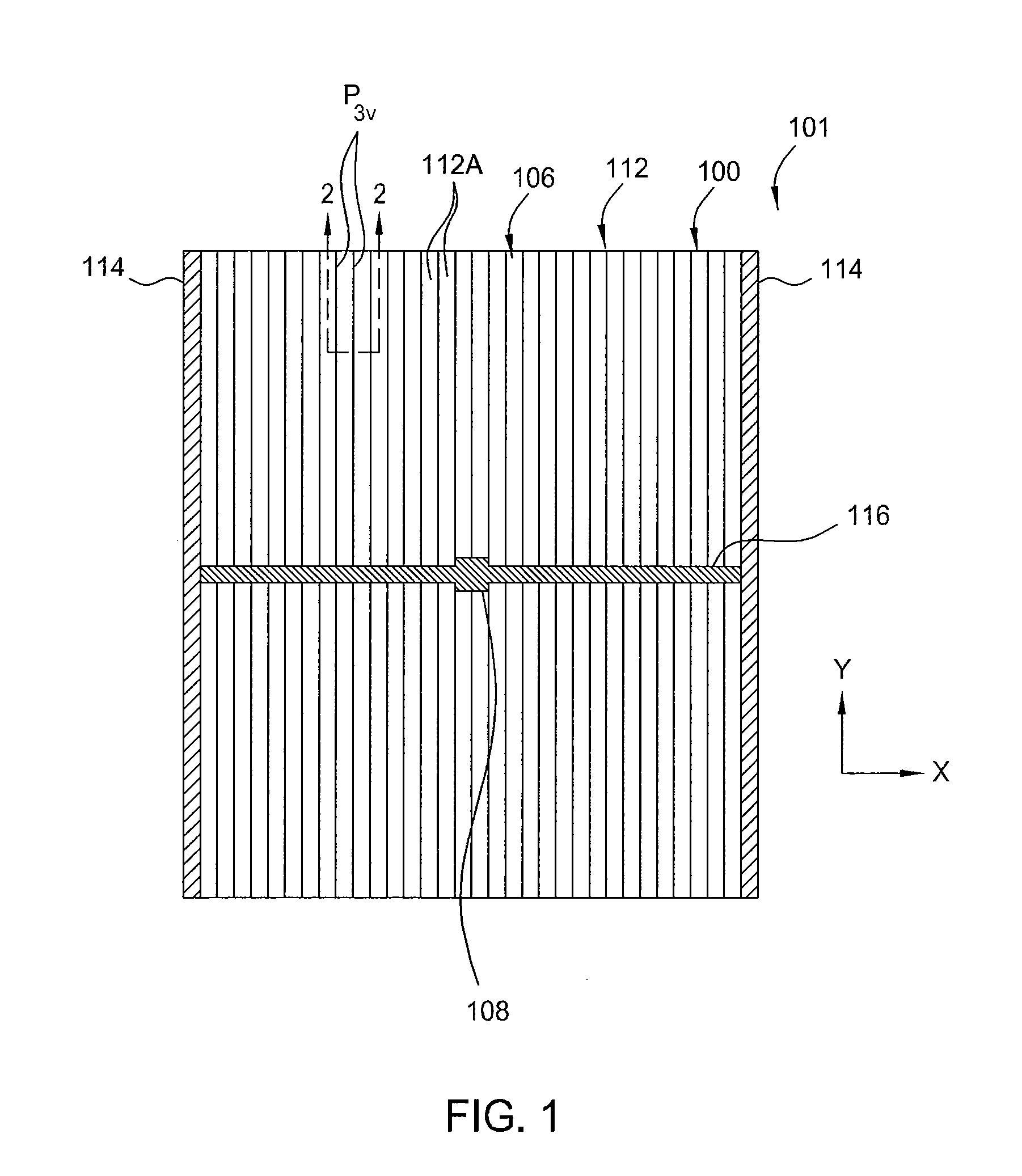
[0022]Embodiments of the present invention relate to the formation of discontinuous gridlines on, beneath or within a transparent conducting oxide (TCO) layer to obtain tunable module voltage and current for thin film photovoltaic devices. The discontinuous gridlines advantageously reduces the effective sheet resistivity of the TCO layer while improving the current conduction of the TCO layer, enabling the use of wider cells to decrease active area loss on the light incident surface while reducing operating voltage almost by half and increasing the operating current without loss in efficiency. Wider solar cells also reduce the number of laser scribes lines that would otherwise required to isolate individual cells from each other when formed with the current standard cell width. With different configurations of the gridlines as discussed below, the module voltage and current of the device are tunable to meet any module performance requirements.

[0023]FIG. 1 depicts a plain view of a s...


PUM


Abstract

A photovoltaic device is provided. In one embodiment, a photovoltaic device includes a transparent conductive oxide (TCO) layer deposited over the substrate, and a plurality of electrical conductive paths disposed in electrical contact with the TCO layer, wherein the plurality of electrical conductive paths extend discontinuously across opposing sides of the substrate.

Description

BACKGROUND OF THE INVENTION[0001]1. Field of the Invention[0002]Embodiments of the present invention generally relate to solar cells and methods for forming the same. More particularly, embodiments of the present invention relate to the formation of discontinuous gridlines on, beneath or within a transparent conducting oxide (TCO) layer to obtain tunable module voltage and current for thin film photovoltaic devices.[0003]2. Description of the Related Art[0004]Solar cells convert solar radiation and other light into usable electrical energy. The energy conversion occurs as the result of the photovoltaic effect. Solar cells may be formed from crystalline material or from amorphous or micro-crystalline materials. Generally, there are two major types of solar cells that are produced in large quantities today, which are crystalline silicon solar cells and thin film solar cells. Crystalline silicon solar cells typically use either mono-crystalline substrates (i.e., single-crystal substrat...

Claims


Application Information

Patent Timeline
IPC IPC(8): H01L31/042H01L31/18
CPCH01L31/022425H01L31/022466Y02E10/548H01L31/1884H01L31/075H01L31/02245
Inventor TANNER, DAVIDLE, HIEN-MINH HUUSU, TZAY-FAWANG, DAPENG
Owner APPLIED MATERIALS INC
Learn More