Interconnection structure

a technology of interconnection structure and electronic apparatus, which is applied in the direction of semiconductor device details, semiconductor/solid-state device devices, instruments, etc., can solve the problems of reducing the number of signal pins, not providing the measurement of signal degradation due to parasitic capacitance of i/o circuit, and not providing performan

Active Publication Date: 2011-07-28
RENESAS ELECTRONICS CORP
View PDF17 Cites 10 Cited by
  • Summary
  • Abstract
  • Description
  • Claims
  • Application Information

AI Technical Summary

Benefits of technology

[0036]The present invention can attain the effect which could not be attained in any conventional techniques, through a distributed constant design by using a phase difference of a transmission signal, and by using a part of a package lead pins for a power supply pin or a ground pin which functions as a return path, and appropriately controlling lengths and intervals of the lead pins.

Problems solved by technology

Also, in the conventional techniques, any measure to signal degradation due to a parasitic capacitance of an I / O circuit is not provided.
As a problem in the conventional techniques, the number of signal pins is reduced, and a method of changing a 2-dimensional structure into a 1-dimensional structure while maintaining desired performance is not provided.

Method used


Image

  • Interconnection structure
  • Interconnection structure
  • Interconnection structure

Examples


first embodiment

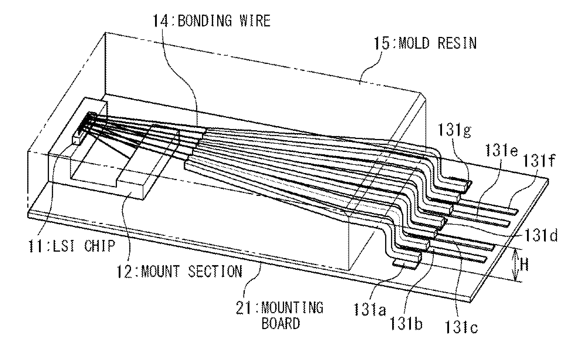
[0063]FIG. 4A is a plan view showing a semiconductor device 10 and a mounting substrate 20 to which the interconnection structure according to a first embodiment of the present invention is applied. FIG. 4B is a sectional view of the semiconductor device and the mounting substrate along the line A-A′ in FIG. 4A.

[0064]The semiconductor device 10 and mounting substrate 20 in FIGS. 4A and 4B will be described. The semiconductor device 10 is provided with an LSI chip 11, a mount section 12, lead pins 131, bonding wires 14 and mold resin 15. Also, the mounting substrate 20 is provided with a mounting board 21 and interconnections 22.

[0065]The LSI chip 11 is mounted on the mount section 12. A plurality of lead pins 131 are arranged around the mount section 12. Connection pads (not shown) of the LSI chip 11 are connected with lead pins 131 or the mount section 12 by bonding wires 14. The mold resin 15 wraps the LSI chip 11, the mount section 12 and a part of the lead pins 131 and the bondi...

second embodiment

[0103]In the second embodiment of the present invention, the same structure as the first embodiment of the present invention is configured on a transmission line substrate such as a printed circuit board. For this purpose, the whole of a lead frame containing a return path is replaced with striplines or micro striplines so as to have a co-planar structure. Although a power supply or a ground is configured as planes in the stripline or the micro stripline, it is required that an aspect ratio of a width and a length is equal to or less than ½, in order to attain the effect of the present invention.

[0104]FIG. 11 is a plan view showing the interconnection structure according to a second embodiment of the present invention. The interconnection structure is provided with a first power supply line 132a, a first differential signal line 132b, a second differential signal line 132c, a second power supply line 132d and bonding wires 14. It is provided with vias 16 in the first and second powe...


PUM


Abstract

An interconnection structure includes: first and second differential signal interconnections provided to transmit a differential signal; and first and second voltage interconnections applied with predetermined voltages. The first voltage interconnection, the first differential signal interconnection, the second differential signal interconnection and the second voltage interconnection are arranged in this order. An interval between the first and second differential signal interconnections is longer than an interval between the first voltage interconnection and the first differential signal interconnection and is longer than an interval between the second differential signal interconnection and the second voltage interconnection. When a first connection point and a second connection point nearest to the first connection point are provided on any of the first and second differential signal interconnections and the first and second voltage interconnections, a distance between the first connection point and the second connection point is in a range of 1/16 of a wavelength of the differential signal to ⅛ of the wavelength thereof.

Description

INCORPORATION BY REFERENCE[0001]This patent application claims a priority on convention based on Japanese Patent Application No. 2010-16444 filed on Jan. 28, 2010. The disclosure thereof is incorporated herein by reference.TECHNICAL FIELD[0002]The present invention is related to an interconnection structure, and especially, to an interconnection structure of an electronic apparatus such as a semiconductor device, and a design method of the interconnection structure.BACKGROUND ART[0003]In recent years, the operation speed of a semiconductor device increases remarkably. Especially, a semiconductor device which can transmit a signal in a high transmission rate of 5 Gbps or more in a low cost is demanded. Accordingly, a semiconductor package and interposer package with high performance in a low cost are required in order to protect the semiconductor chip and to connect with a system board.[0004]The interposer package which is provided with a stripline or a micro stripline in many printe...

Claims


Application Information

Patent Timeline
Patent Type & Authority Applications(United States)
IPC IPC(8): H01L23/538G06F17/50
CPCH01L23/66H01L2224/48091H01L2224/48247H01L2924/3011H01L23/49503H01L23/49541H01L24/48H01L2924/01067H01L2924/30107H01L2924/3025H01L2223/6638H01L2224/49171H01L2224/73265H01L2924/00014H01L2924/00H01L24/49H01L2224/49433H01L2924/30111H01L2224/45099H01L2224/45015H01L2924/207
Inventor OIKAWA, RYUICHI
Owner RENESAS ELECTRONICS CORP
Why Eureka
Try Eureka