Non-volatile memory low voltage and high speed erasure method

Active Publication Date: 2011-07-28
YIELD MICROELECTRONICS CORP
View PDF3 Cites 4 Cited by
  • Summary
  • Abstract
  • Description
  • Claims
  • Application Information

AI Technical Summary

Benefits of technology

[0007]Another objective of the present invention is to provide a non-volatile memory low voltage and high speed erasure method, wherein, positive and negative voltages are

Problems solved by technology

In a structure of non-volatile memory of the prior art, usually, the erasure voltage utilized is in the excess of 10V, and the time required for erasure is in the order of milli-second (ms), such that not only the voltage raising area could cause the increase of cost, but it also can not achieve the purpose of low voltage and hig

Method used


Image

  • Non-volatile memory low voltage and high speed erasure method
  • Non-volatile memory low voltage and high speed erasure method
  • Non-volatile memory low voltage and high speed erasure method

Examples


first embodiment

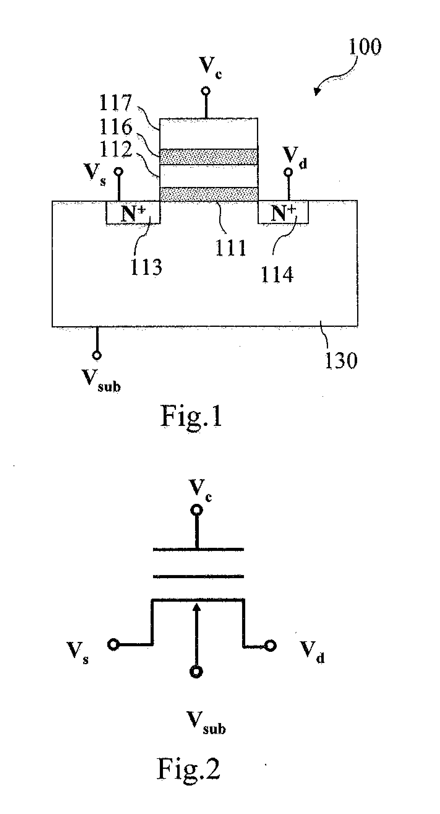
[0019]Refer to FIG. 1 for a cross section view of a non-volatile memory structure according to the present invention. As shown in FIG. 1, the non-volatile memory structure 100 includes: a stacked gate structure disposed in a P-type semiconductor substrate 130. The stacked gate structure includes: a floating gate 112 stacked on a tunneling dielectric layer 111, a control gate 117 disposed above the floating gate 112 through a gate dielectric layer 116, and a source 113 and a drain 114 disposed in a P-type semiconductor substrate 130. Wherein, the source 113 and the drain 114 are N-type ion-doped regions.

[0020]As shown in FIG. 1, the non-volatile memory structure 100 is a structure having four terminals: a source, a drain, a controlling gate, and a substrate connection structure respectively, such that a substrate voltage Vsub, a source voltage Vs, a drain voltage Vd, and a control gate voltage Vc are applied on the substrate 130, the source 113, the drain 114, and the control gate 11...

second embodiment

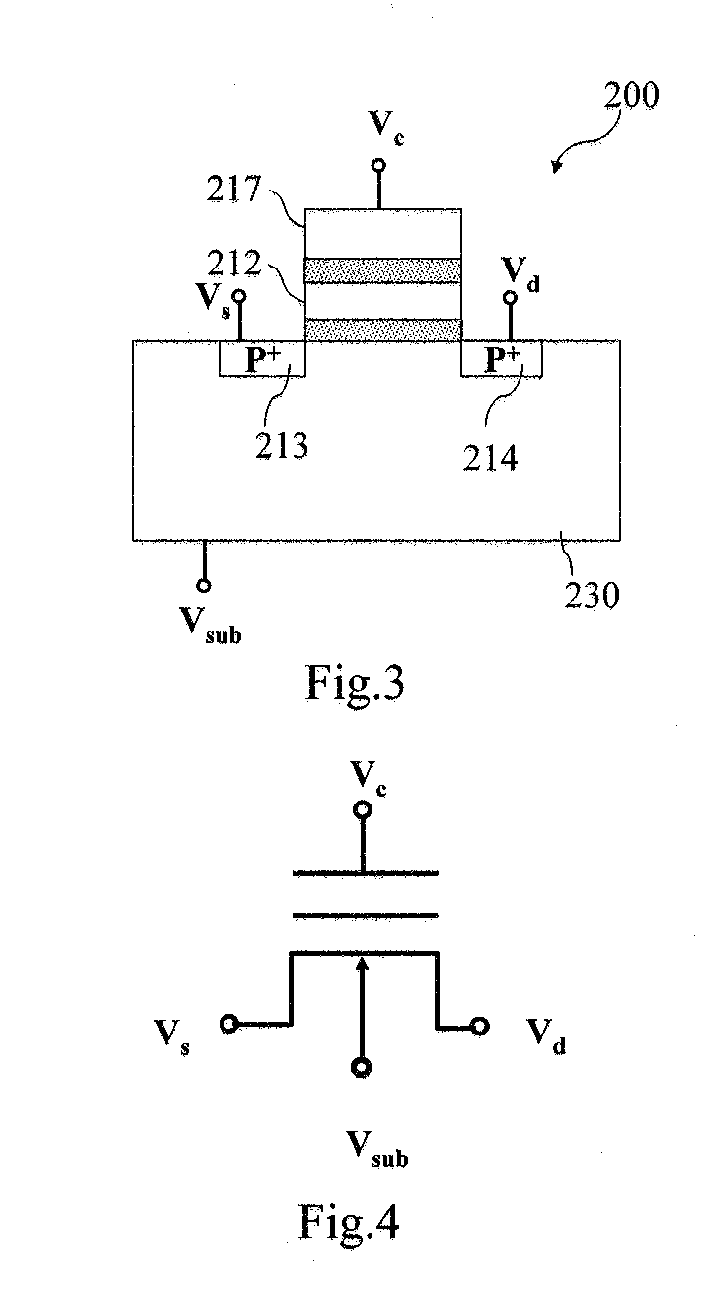
[0028]FIG. 3 is a cross section view of a non-volatile memory structure according to the present invention. As shown in FIG. 3, the non-volatile memory structure 200 of the present invention can be realized through forming a stacked gate structure in an N-type semiconductor substrate 230, such that the source 213 and the drain 214 are P-type ion-doped regions, and the stacked gate structure includes a control gate 217 stacked above a floating gate 212.

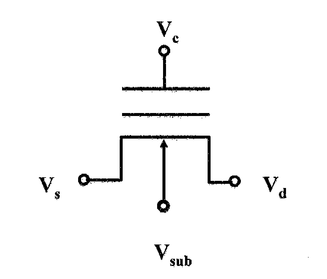
[0029]In performing low voltage and high speed erasure process to the non-volatile memory structure 200, the erasure is achieved through applying substrate voltage Vsub, source voltage Vs, drain voltage Vd, and control gate voltage Vc on the substrate 230, the source 213, drain 214, and the control gate 217 respectively. FIG. 4 is an equivalent circuit diagram of a non-volatile memory structure of FIG. 3 according to a second embodiment of the present invention, such that the operation conditions of the low voltage and high speed erasu...

third embodiment

[0034]FIG. 5 is a cross section view of a non-volatile memory structure according to the present invention. As shown in FIG. 5, the non-volatile memory structure 300 of the present invention can be realized through forming a stacked gate structure in an N-type semiconductor substrate 330, such that the source 313 and the drain 314 are P-type ion-doped regions, a P-type well is provided underneath the source 313 and the drain 314, and the stacked gate structure includes a control gate 317 stacked above a floating gate 312.

[0035]In performing low voltage and high speed erasure process to the non-volatile memory structure 300, the erasure is achieved through applying substrate voltage Vsub, P-type well voltage Vpwell, source voltage Vs, drain voltage Vd, and control gate voltage Vc on the substrate 330, the P-type well 316, the source 313, the drain 314, and the control gate 317 respectively, such that the operation conditions of the low voltage and high speed erasure process of the no...


PUM


Abstract

A non-volatile memory low voltage and high speed erasure method, the non-volatile memory is realized through disposing a stacked gate structure having a control gate and a floating gate on a semiconductor substrate or in an isolation well, such that adequate hot holes are generated in proceeding with low voltage and high speed erasure operation through a drain reverse bias and making changes to gate voltage. In addition, through applying positive and negative voltages on a drain, a gate, and a semiconductor substrate or well regions, adequate hot holes are generated, so as to lower the absolute voltage in achieving the objective of reducing voltage of erasing memory.

Description

BACKGROUND OF THE INVENTION [0001]1. Field of the Invention[0002]The present invention relates to a non-volatile memory low voltage and high speed erasure method, and in particular to a non-volatile memory low voltage and high speed erasure method, that can be used to generate adequate hot holes to proceed with low voltage and high speed erasure operations by means of reverse bias and changed gate voltage.[0003]2. The Prior Arts[0004]Presently, Complementary Metal Oxide Semiconductor (CMOS) technology is frequently utilized in producing Application Specific Integrated Circuit (ASIC), and in the present age of Computer & Information technologies, the Electrically Erasable Programmable Read Only Memory (EEPROM) is widely utilized in various electronic products for its non-volatile memory capability of being electrically programmable and erasable, and also data stored therein will not disappear after power is shut down.[0005]In general, the non-volatile memory is programmable, that can...

Claims


Application Information

Patent Timeline
IPC IPC(8): G11C16/04H01L29/788
CPCG11C16/0416H01L29/7885G11C16/3418G11C16/14
Inventor LIN, HSIN CHANGHUANG, WEN CHIEN
Owner YIELD MICROELECTRONICS CORP
Why Eureka
Try Eureka